Device fabrication
Our laboratory is equipped with a unique set of facilities for the III-nitride device fabrication. These include:
- A STS Multiplex Plasma Enhanced Chemical Vapor Deposition (PECVD) system which is used for the deposition of high quality dielectric mirrors and passivation layers, etc.
- A production scale e-beam evaporation system for the deposition of metal contacts as well as dielectric materials.
- A research scale e-beam evaporation system for the deposition of metal contacts as well as dielectric materials.
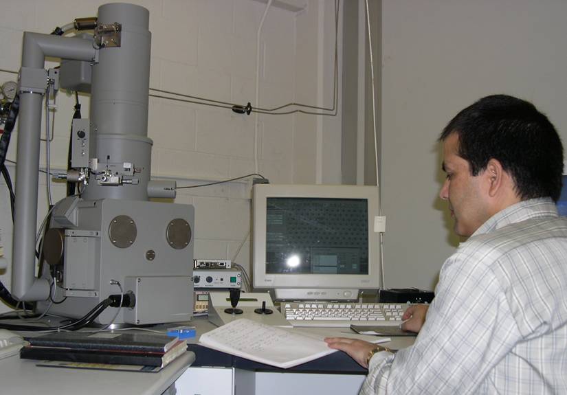
- SEM (LEO-440) based e-beam lithography system for nano-scale device patterning with a line resolution of about 30 nm (60 nm) for conducting (insulating) substrate.
- A deep UV photolithography systems for sub-micron device patterning (0.25 micron line resolution).
- Plasma-Therm Series 790 Inductively Coupled Plasma (ICP) etching system for dry etching and device pattern transfer.
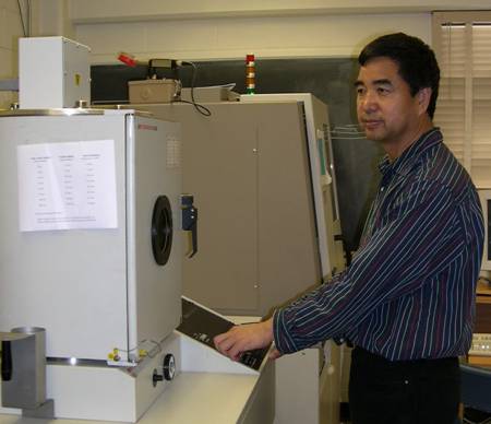
- Single-wafer rapid thermal annealing furnace (reaches 1200 C in 5 seconds).
- Multi-wafer thermal annealing furnace (up to 900 C).
- High temperature thermal annealing furnace (up to ~1900 C).
- A laser-lift-off (LLO) system for sapphire substrate removal. A unique feature of our LLO system is that it is able to remove the whole 2” wafers aligning free.
- Flip-chip bonding system (RD Automation) is used for device packaging and for bump-mounting individual or arrays of devices onto sub-mounts or other driving/read-out circuits.
- Automated wafer scribe/dicing system (Dynatex).
- Sapphire wafer lapping/polishing systems.
- Pulse source meters, LED and laser diode drivers.
- Probe stations, wire bonders, micromanipulators, optical microscopes with digital cameras for LED and laser diode characterization.
- Tektronix programmable curve tracer and 45 GHz analog and digital oscilloscopes.
- Ocean Optics spectrometers for electroluminescent emission characterization for deep UV, UV, and visible emitters.
- High sensitivity spectrometers for electroluminescent emission characterization of IR emitters.
- Optical transmission/reflectance spectroscopy measurement setup.
- Standard AM1.5 solar simulator for determining external efficiencies of various solar cells.
Safety Operation Procedures
Check this page before operation on our lab facilities to protect both you and our safety