material growth - Metal-Organic Chemical Vapor Deposition (MOCVD)
full view of MOCVD room
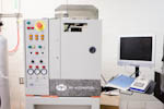
MOCVD machine #1
MOCVD machine #2
MOCVD machine #3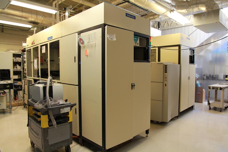
MOCVD machine #4 and #5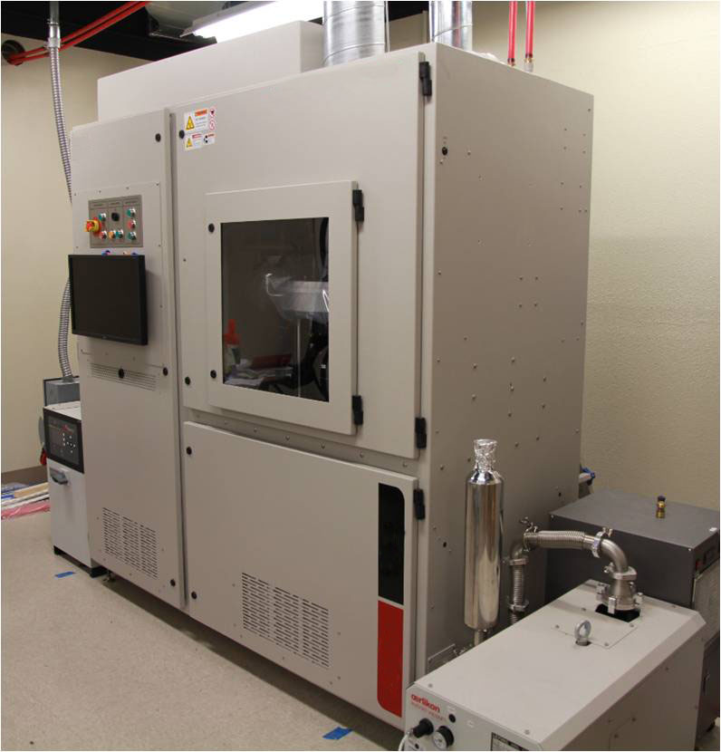
MOCVD machine #6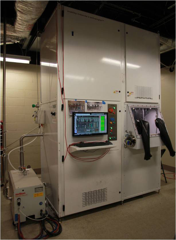
HVPE
)
)
)
)
)
)
)
characterization
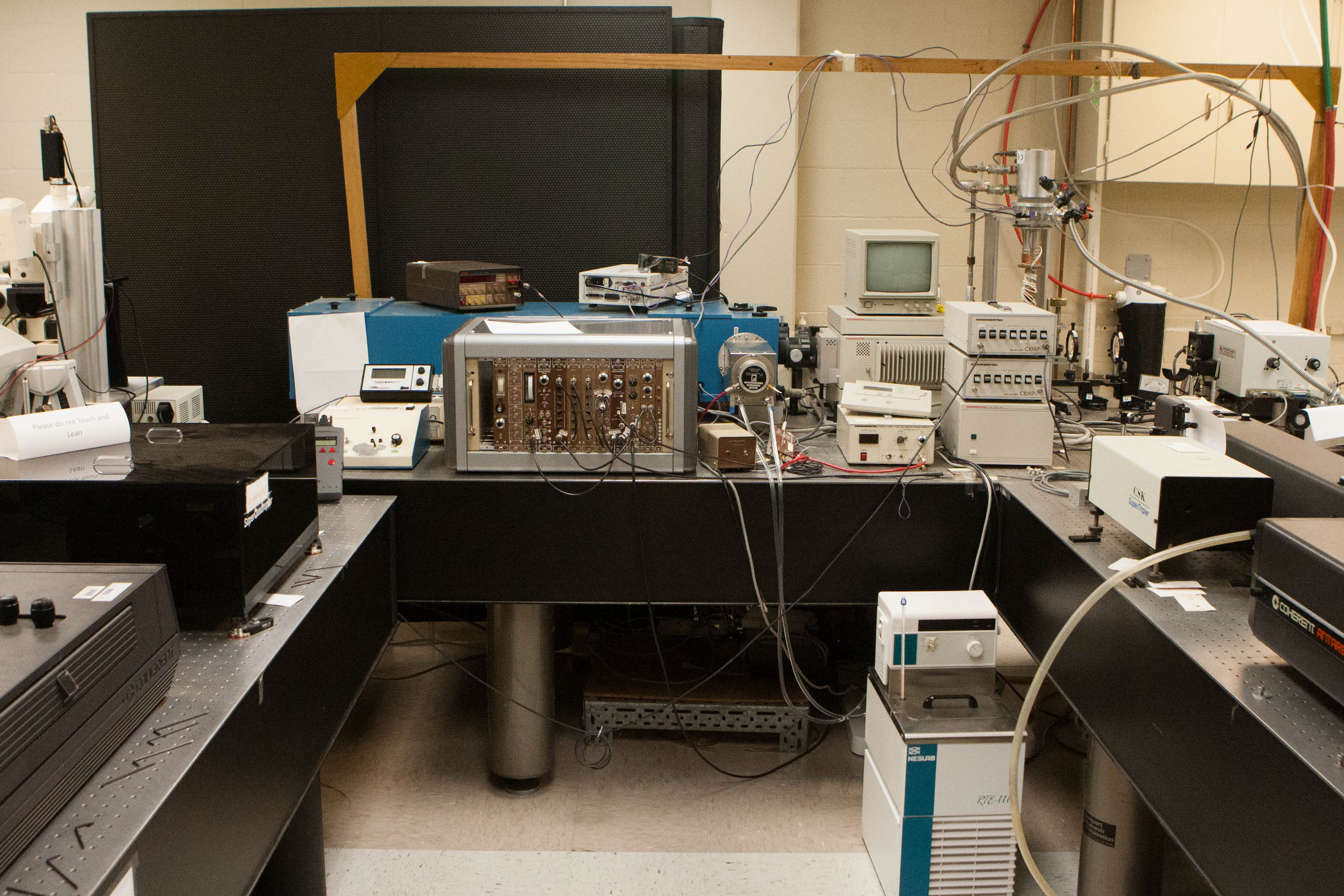
PL measurements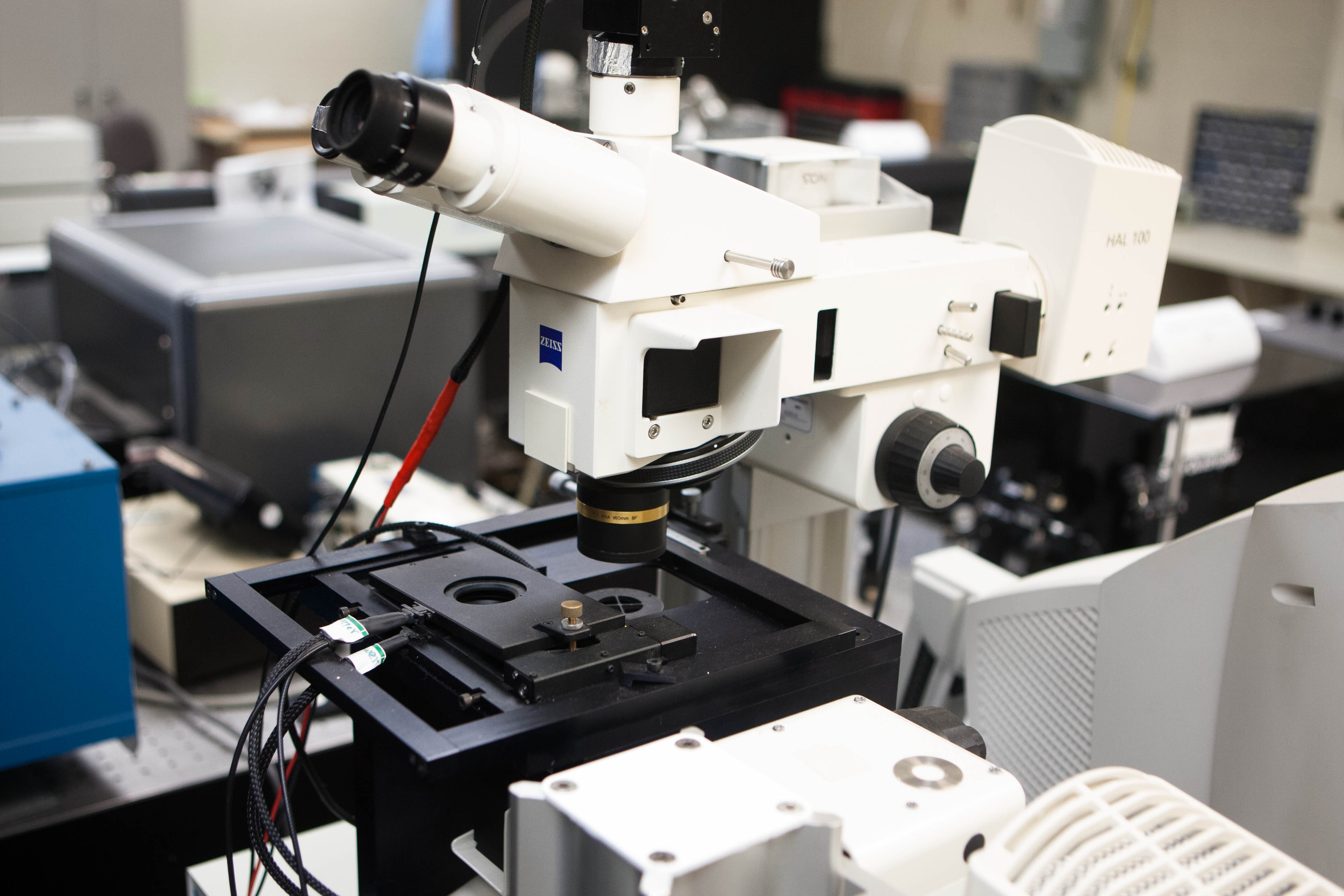
NSOM
AFM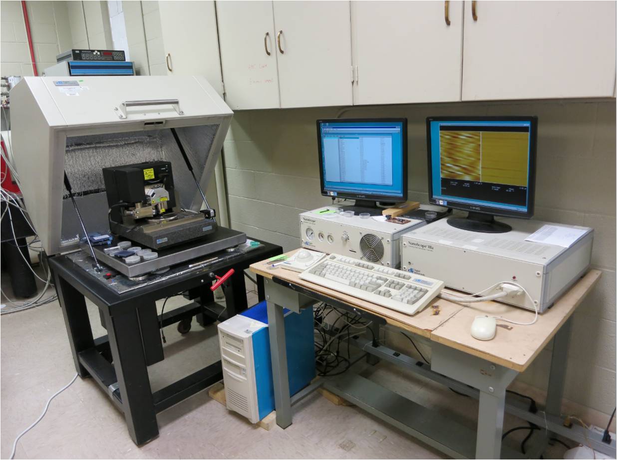
High-resolution AFM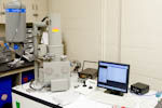
SEM and e-beam lithography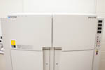
X-ray mapping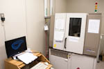
X-ray Diffraction (XRD)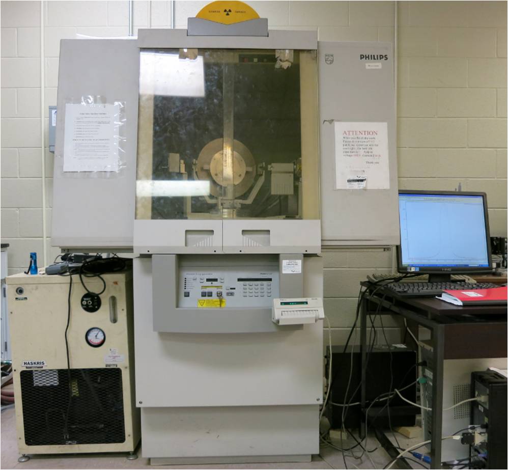
High-resolution XRD
Hall effect measurement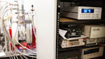
electrical conductivity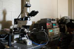
probe stations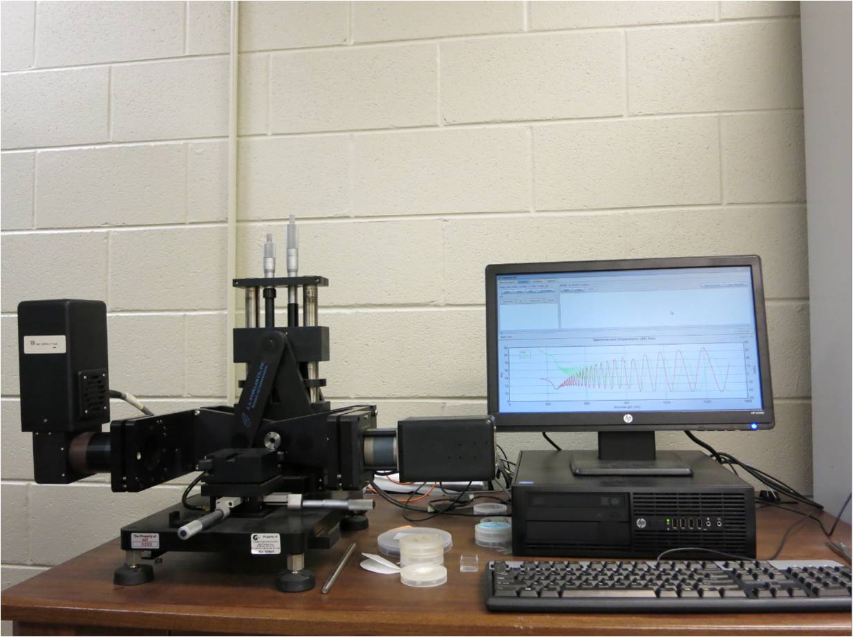
Spectroscopic ellipsometer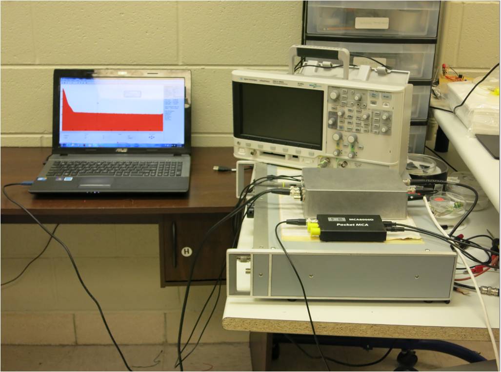
Neutron detector calibration.jpg)
Thermal neutron source
)
','NSOM.jpg',800,600,''))
','AFM.jpg',800,600,''))
)
','SEM.jpg',800,600,''))
)
','X-ray system.png',800,600,''))
)
)
)
)
)
)
','Thermal Neutron Source (252Cf in HDPE moderator).jpg',600,450,''))
Flip Chip Bonding machine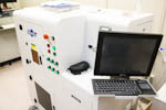
Laser lift-off machine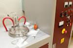
high temperature annealing machine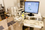
ICP etching machine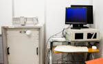
PECVD machine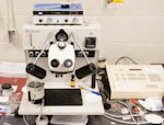
wire bonding machine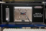
RTA furnace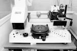
deep UV photolithography machine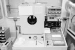
e-beam evaporator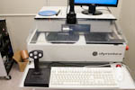
wafer dicing system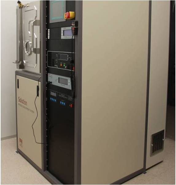
Large-scale e-beam evaporation
)
)
)
 etching','ICP.jpg',800,600,'a Plasma-Therm Series 790 ICP dry etching system'))
','PECVD.jpg',800,600,'PECVD is used to deposit dielectric materials.'))
)
','RTA.jpg',800,600,''))
)
)
)
)
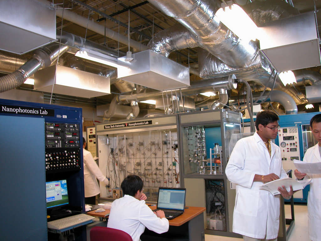
This page links to all the state-of-the-art facilities that the Nanophotonics Center at TTU utilizes in their research. Please follow the links to get information and photographs of our research and progress.