
Our group’s research is dedicated to the advancement of nitride wide bandgap semiconductors (GaN, AlN, AlGaN, InGaN, and InAlGaN). There are three main areas.
Materials growth
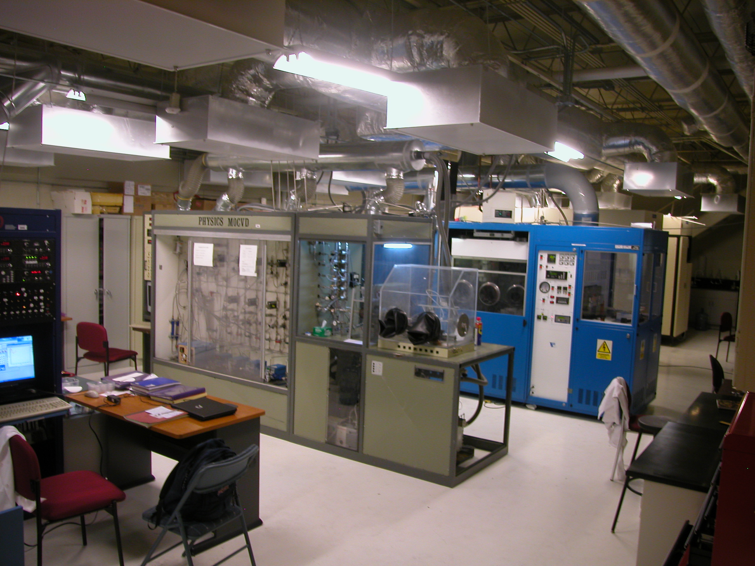
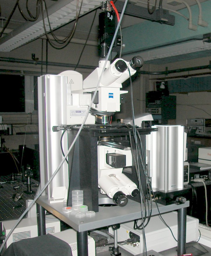
Our focus is to optimize MOCVD growth conditions for III-nitrides, particularly for BN as well as AlGaN and InGaN ternary alloys with high Al and In contents, including pure AlN and InN. New methods to further reduce crystal defect density and enhanced doping efficiency will be explored. Because of our unique materials characterization capabilities, we are equipped with “eyes” for monitoring the material quality as well as for probing the fundamental optical properties of a wide range of semiconducting materials.
Optical studies
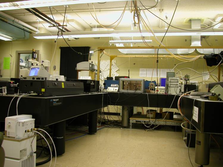
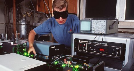
Our objectives are to investigate the mechanisms of optical transitions, light emitting diode emission, and lasing in nitride materials, to understand the fundamental optical transitions and dynamic processes, to study the physics components of nitride based optoelectronic devices, and to provide input for new approaches toward the improvement of materials quality and the optimization of optoelectronic devices.
Device fabrication and characterization
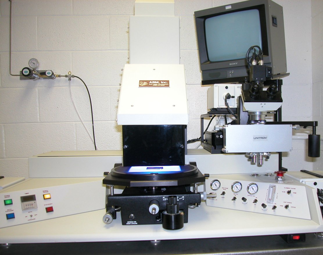
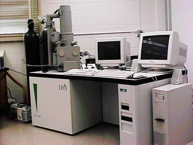
Our focus is to further develop innovative methods for fabricating micro- and nano-scale photonic structures and devices based III-nitrides. Currently, we are exploring III-nitrides for applications of solid-state lighting and energy-conversion devices, and optical communications. We are also interested in further developing technologies for fabricating solid-state radiation sensors.
Also see “News” section for media reports
Safety Operation Procedures
Check this page before operation on our lab facilities to protect both you and our safety