Research:
Our ongoing work embodies a commitment to excellence in advancing the frontiers of III-nitride (BN, GaN, AlN, AlGaN, InGaN, and InAlGaN) semiconductor material and device technologies. These materials have contributed on the grandest scale to many technological advances including UV/blue/green/white LEDs, solid-state lighting, UV/blue/green laser diodes, UV/visible detectors, and high temperature/power transistors. Our group’s concentration areas are epitaxial growth, micro- and nanostructure and device fabrication, and fundamental optical and transport properties investigations. Our work has resulted in numerous “Firsts”:
· Invented MicroLED in 2000 – The invention created the microLED display industry and the microLED research field. See Hongxing Jiang, Jingyu Lin, Sixuan Jin, and Jing Li, “Micro-size LED and detector arrays for mini-displays, hyperbright light emitting diodes, lighting, and UV detector and imaging sensor applications,” US patent 6,410,940; US patent 8,058,663, Sixuan Jin, Jing Li, Jizhong Li, Jingyu Lin and Hongxing Jiang, “GaN microdisk light emitting diodes," Appl. Phys. Lett. 116, 100502 (2000); S. X. Jin, J. Li, J. Y. Lin, and H. X. Jiang, “InGaN/GaN quantum well interconnected microdisk light emitting diodes,” Appl. Phys. Lett. 77, 3236 (2000). Hongxing Jiang, Sixuan Jin, Jing Li, Jagat Shakya, and Jingyu Lin, “III-Nitride Blue Microdisplays” Appl. Phys. Lett. 78, 1303 (2001); S. X. Jin, J. Shakya, J. Y. Lin, and H. X. Jiang, “Size dependence of III-nitride microdisk light emitting diode characteristics,” Appl. Phys. Lett. 78, 3532 (2001); Hongxing Jiang and Jingyu Lin, “How we made the microLED,” Nature Electronics 6, 257 (2023);News
· Developed in 2009 the first active-driven full-scale high resolution microLED microdisplay – This VGA microLED microdisplay (640 x 480 pixels, pixels size 12 mm and pixel pitch 15 mm) capable of playing video graphics images was produced by integrating microLED array and Si CMOS. US patent 9,047,818 (Priorities: US31675509P·2009-03-23; US201113046725A·2011-03-12); Jacob Day, Jing Li, Donald Lie, Charles Bradford, Jingyu Lin and Hongxing Jiang, Appl. Phys. Lett. 99, 031116 (2011); Jingyu Lin, Jacob Day, Jing Li, Donald Lie, Charles Bradford, and Hongxing Jiang, "High-resolution group III nitride microdisplays" SPIE Newsroom Dec issue (2011) PDF.
· Invented in 2002 high-voltage AC/DC-LEDs via on-chip integration of micro- and mini-LED arrays. This invention extended LED’s operating voltage from 2 or 3 V DC up to 100’sV AC. Hongxing Jiang, Jingyu Lin and Sixuan Jin, US patent 6957899. US patent 7,221,044. US patent 7,535,028. US patent 8,272,757. US patent 7,714,348. Technology has been commercialized worldwide for general lighting in homes and automobiles.
·
Developed
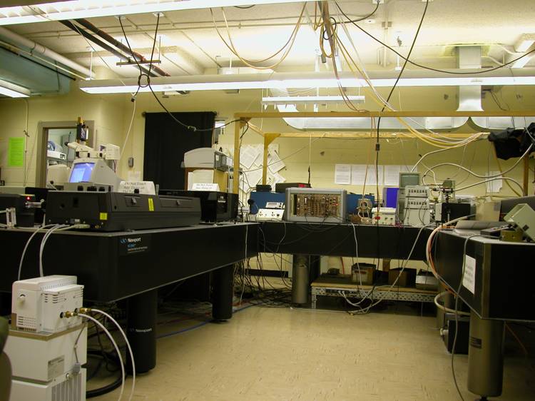
the first deep UV picosecond time-resolved optical spectroscopy system
(down to 195 nm). The system is capable to probe the static and
dynamic recombination processes in semiconductors with ultrawide bandgaps
with a ps time resolution. The design has been adopted by the photonic
industries to benefit the research communities at large
and helped the field to characterize and advance ultrawide bandgap
semiconductors. See e.g.,
Appl. Phys. Lett. 81, 3365
(2002);
PDF
·
One of the first to experimentally determine the Mg acceptor energy level
in AlN
– Optically:
Appl. Phys. Lett. 83,
878 (2003); by
Hall-effect:
Appl. Phys. Lett. 89, 152120
(2006).
·
Realized the 1st GaN photonic crystal LED -
Appl. Phys. Lett. 83, 1231 (2003);
Appl. Phys.
Lett. 84, 466 (2004).
· First to predict/demonstrate that AlN is an edge-emitter (light emission in TM mode, Eemi//c) - The TM mode is the dominant laser emission in UV laser diodes (LDs) using high Al-content AlGaN as active layers, in contrast to all other semiconductor LDs in which the TE mode is the dominant lasing emission. – Appl. Phys. Lett. 84, 5264 (2004); Appl. Phys. Lett. 83, 5163 (2003).
· Among the first to achieve conductivity control in Al-rich AlGaN and AlN – r(AlN:Si)=12 W×cm (n=2x1017 cm-3, m=4 cm2/V×s) @300 K in Appl. Phys. Lett. 85, 3769 (2004) and r( Al0.7GaN0.3N:Si)=0.0075W×cm (n=3.3x1019 cm-3, m=25 cm2/V×s) @300 K in Appl. Phys. Lett. 85, 4669 (2004); r(Al0.7GaN0.3N:Mg)=40 W×cm @800 K in Appl. Phys. Lett. 86, 092108 (2005); r(AlN:Mg)=450 W×cm @850 K in Appl. Phys. Lett. 89, 152120 (2006).
· Among the first to exploit III-nitrides for solid-state energy devices - Demonstrated the first InGaN quantum well solar cell for improved solar conversion efficiency, Appl. Phys. Lett. 94, 063505 (2009);Ι PDF Ι News; InGaN photoelectrochemical cells for hydrogen generation and energy storage, Appl. Phys. Lett. 96, 052110 (2010); Thermoelectrics based on InGaN and InAlGaN alloys for converting waste heat to electricity; Appl. Phys. Lett. 92, 042112 (2008) PDF
· Achieved the first integration of Er doped GaN 1.5 micron LED with CMOS compatible Si (100) substrates for Si photonics and optical communications; Appl. Phys. Lett. 97, 141109 (2010) Ι PDF; Appl. Phys. Lett. 98, 081102 (2011) PDF Ι News
· Successfully fabricated the first blue LED on 6-inch Si substrate; Appl.
Phys. Lett. 88, 171909 (2006), PDF Ι News
· Pioneered the development of h-BN neutron detectors. Our research group has achieved h-BN thermal neutron detectors with a record high detection efficiency (at 60% to date) - Appl. Phys. Lett. 109, 072101 (2016); Appl. Phys. Lett. 111, 033507 (2017); J. Appl. Phys. 123, 044501 (2018); Appl. Phys. Lett. 116, 142102 (2020); J. Appl. Phys. 135, 175704 (2024). News; News
· We are the only group in the world possessing the capability for synthesizing large diameter h-BN quasi-bulk crystals with wafer size up to 6” in diameter and thickness up to 1 mm (see. e.g., Appl. Phys. Lett. 122, 012105 (2023); J. Appl. Phys. 135, 175704 (2024).
·
Professor Hongxing Jiang and Professor
Jingyu Lin are co-founders 3N and AC-LED. The companies hold patent
portfolios and facilitated the commercialization of microLED display
and single-chip high voltage AC/DC LED technologies.
Our current research is supported by DOE (ARPA-E)
1. "Ultrawide band gap semiconductors for
extrinsic photoconductive switching devices," ARPA-E
ULTRAFAST program
2. "Development of cubic boron nitride (c-BN)
ultrawide bandgap semiconductors," ARPA-E
CREATE program
Professor Hongxing Jiang and Professor Jingyu Lin were the team members of the following research programs:
Joint Directed Energy Transition Office (DE-JTO)
MRI program via Air Force Research Laboratory/Office of Naval
Research
DOD-JTO/AFRL (Beam
Control Research and Development
program)
BMDO GAMPA Program
DARPA SUVOS Program
DARPA VIGIL Program
DARPA DUVAP Program
DARPA CMUVT Program
DHS (ARI Research Program)
Our research was also supported by
DOE (BES and NNSA)
ARO
NSF
The founding of the TTU Nanophotonics Center would
not have been possible without the support of
Mr. Ed Whitacre and the AT
& T Foundation.
Contact Information:
Dr. Hongxing Jiang, Ed Whitacre Endowed Chair and Horn Professor
hx.jiang@ttu.edu
Dr. Jingyu Lin, Linda Whitacre Endowed Chair and Horn Professor
Jingyu.lin@ttu.edu
Dr. Jing Li, Research Professor
Jing.li@ttu.edu
Postal address:
Nanophotonics Center
Engineering and Technology Lab Building
Texas Tech University
901 Boston Ave
Lubbock, TX 79409


