
Ultraclean Silicon Surfaces
H. Temkin and S. A. Nikishin
An essential goal to extending the silicon technology roadmap is the development of new gate dielectric materials to replace the venerable silicon dioxide. Successful materials must have high dielectric constant compared to SiO2 , be thermodynamically stable with respect to silicon, and be compatible with high temperature silicon processes. However, the propensity for silicon to oxidize, even by scavenging oxygen from surrounding stable compounds, makes it extremely challenging to produce a new dielectric material without also forming a SiO2 layer. Recent work conducted at Texas Tech University on hafnium oxide, HfO2, has illustrated the value of low temperature methods by demonstrating a gate stack with the equivalent oxide thickness of 0.5 nm for a 3 nm film thickness. Critical to the success of this approach has been surface analysis of the efficacy of conventional cleaning processes to unintentional SiO2 formation.
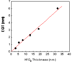
Equivalent oxide thickness plotted as a function of the physical thickness of HfO2
Formation of atomically clean silicon surfaces, prior to subsequent deposition, is crucial to successful formation of a high-k gate dielectrics. A modified Shiraki etch was found to be highly effective and reproducible. The cleaning procedure starts with the removal of native oxides followed by the growth of a thin controlled oxide layer. The last step of this process consists of HF:ethanol treatment. Replacement of H2O, used in the standard RCA clean, with ethanol inhibits formation of Si-F bonds at the surface, leaving a flat surface terminated with H. This surface is immune to re-oxidation for several hours.
Low energy electron diffraction (LEED) is used to compare silicon surfaces prepared with Shiraki and RCA cleans. The contrast between sharp, distinct diffraction spots of Shiraki clean, obtained at a low bias of 26 V, and relatively diffused spots of RCA, at 60 V, lead us to conclude that the latter is composed of partially cleaned domains and is rougher. Once a clean surface is prepared, intentional oxidation or nitridation can be performed and the process monitored in-situ.
HfO2 layers are prepared on p-type Si(100) passivated using the Shiraki method. Test capacitors were formed on high-K layers by evaporating titanium contacts followed by hydrogen annealing. We observe negligibly small hysteresis and frequency dependence. The dielectric constant of the bulk was found to be K = 21.5 ± 0.6 The associated SiO2 interface layer is 0.04 nm thick. These results suggest minimal interface layer formation, consistent with our LEED studies.
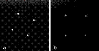
(1x1) LEED images of Si(100); (a) Shiraki clean: 26V, and (b) RCA clean: 60V.
Research Support: SEMATECH, NSF
Nano Tech Center
-
Address
Texas Tech University | Whitacre College of Engineering -
Phone
806.742.3533 -
Email
webmaster.coe@ttu.edu