
Controlled Growth of GaN Nanowires
H. Temkin and M. Holtz
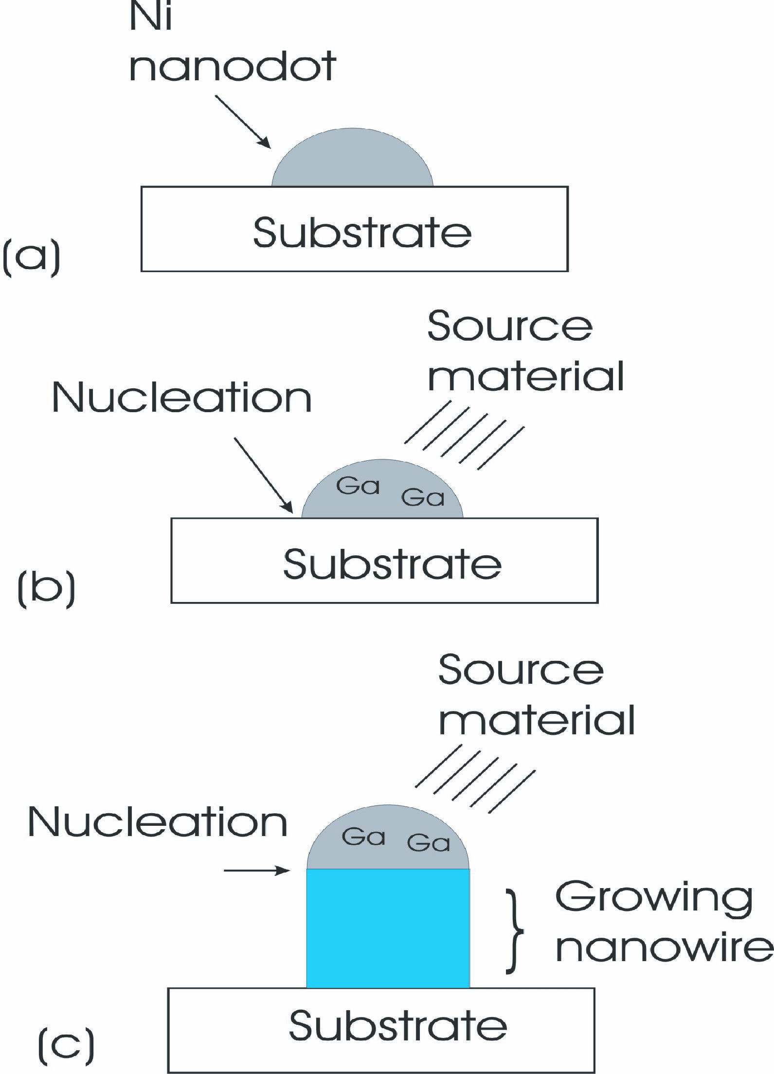
Semiconductor nanowires are quasi-one-dimensional structures exhibiting unique electrical and optical properties. The purpose is to obtain highly perfect wires, free of dislocations, in order to explore the intrinsic optical and electrical properties of technologically important materials and the possibility of novel devices based on 1D structures. One of the approaches to formation of nanowires is the vapor-liquid-solid (VLS) method. The process, as illustrated here, starts with self-assembly of nanodots of a metal catalyst, e.g. Ni on a substrate such as Si(111) or sapphire (0001). Once the heat treatment required for the metal self-assembly is completed, the metal (or molten eutectic) is exposed to source materials, e.g. Ga and active nitrogen, delivered in vapor form, and supersaturated with them. The source material is diffused from the vapor-liquid to the liquid-solid interface. Precipitation of the material at the liquid-solid interface drives the growth of the wire directly under the metal nanodot, with the metal droplet riding over the growing wire. The size of growing nanowires, and their density, is controlled by the size and density of metal nanodots.
Our nanowire growth begins with a ~ 2 nm thick layer of Ni deposited on substrate sapphire. Annealing at high temperatures causes the Ni to self assemble into regular nanodots. By controlling the diameter of these nanodots, we control the diameter of the nanowires. Furthermore, the growth time allows us to control the nanowire length.
Semiconductor Nanowires
A representative composite scanning electron microscope image of GaN nanowires is shown on the right. The nanowires grow perpendicular to the substrate, with fairly constant diameters, smooth sidewalls, and hexagonal cross-sections. Nanowires grow selectively from islands of the metal catalyst and no deposits of GaN could be seen between the wires. A slight increase in the diameter of the growing wire, visible in Fig. 7(a), may be indicative of sidewall growth. Characteristic metal caps at nanowires tips, shown in the inset (b) of Fig. 7, confirm the VLS growth mechanism. The shape of the caps is typical of Ni nanodots formed in high temperature, 830oC, anneals.
Research support: NSF
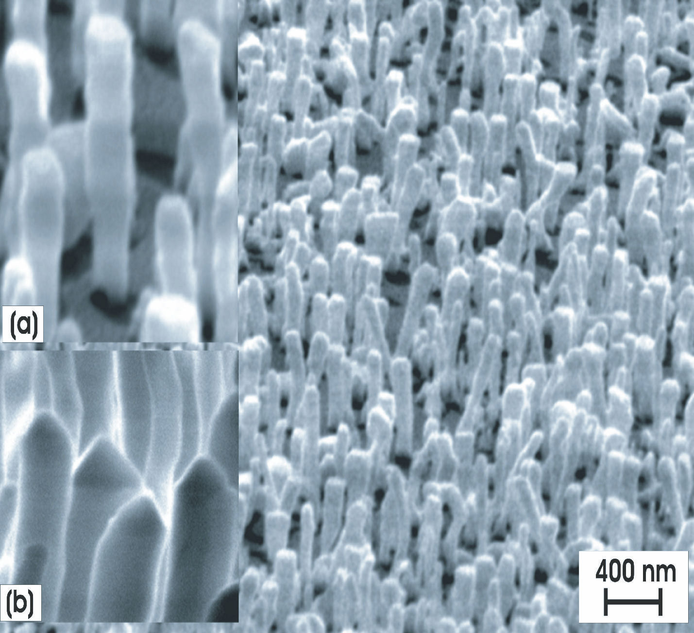
SEM Image of GaN Nanowires
Nano Tech Center
-
Address
Texas Tech University | Whitacre College of Engineering -
Phone
806.742.3533 -
Email
webmaster.coe@ttu.edu