
Ultraviolet Light Emitting Diode (UV-LED)
S. Nikishin, B. Borisov, G. Kipshidze, V. Kuryatkov, M. Holtz, and H. Temkin
Light emitting diodes producing blue light have been considered impossible in the past. This was because the bandgap of known semiconductors was too small to produce light in this spectral region. Nobody thought of preparing LEDs with a shorter wavelength emission, in the ultraviolet. Such light sources would make is possible to develop a range of new applications, from CDs with ultra-high capacity, to fluorescent excitation sources for biodetection, and ever replacement of conventional light bulbs. The development of nitride-based semiconductors has changed all that.
We are now capable of preparing deep ultraviolet LEDs operating in the spectral range of 250-290 nm. These devices are grown by molecular beam epitaxy with ammonia as a source of active nitrogen. We use sapphire substrates, transparent in this wavelength range, on which a layer of AlN is grown first. It is followed by a buffer layer of ternary alloy AlGaN with the Al concentration greater than 0.60, also transparent in the UV. The device structure grown over the buffer layer consists of three major parts: the n-type cladding layer (the source of electrons), the active region, and the p-type cladding layer (the source of holes). A thin contact layer of p-GaN terminates the structure.
The properties of all layers forming the device must be carefully adjusted to produce the desired optical and electrical properties. The n-type cladding layer is doped with Si to a level as high as 10 19 cm -3 to assure low resistance of the LED.
The properties of all layers forming the device must be carefully adjusted to produce the desired optical and electrical properties. The n-type cladding layer is doped with Si to a level as high as 10 19 cm -3 to assure low resistance of the LED. The active region is formed of three to five quantum undoped wells of AlGaN, separated by barriers of AlN. The wells are typically two to three atomic layers thick (0.5 to -0.75 nm). The barriers have similar thickness of 1.0-1.25 nm. Under forward bias, electrons and holes from the n-type and p-type cladding layers, respectively, recombine in the wells generating ultraviolet light. The p-type cladding layer is the most difficult to prepare. Only a very small fraction of Mg, the commonly used p-type dopant, becomes electrically active in layers of AlGaN needed to form the cladding layer and this fraction becomes smaller as the Al content increases. It is thus not possible to prepare p-type cladding layers of AlGaN with the required hole concentration on the order of 10 18 cm -3. We have solved this problem by substituting the random alloy with a digital alloy formed by alternating layers of GaN and AlN. The average alloy composition remains unchanged, with the Al content greater than 0.60. This is done by keeping individual layers very thin, in the range of 2-5 atomic layers. Mg is introduced in GaN, in which its activation is relatively effective and holes can move through thin AlN barriers by quantum mechanical tunneling.
Research Support: DARPA, SBCCOM, NSF
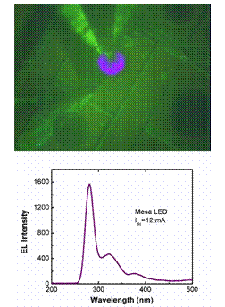
Light emitting region of a UV-LED and the spectrum of light emitted by such a device.
Nano Tech Center
-
Address
Texas Tech University | Whitacre College of Engineering -
Phone
806.742.3533 -
Email
webmaster.coe@ttu.edu