
Nano-Engineered Surfaces and Interfaces
M. Holtz, J. M. Berg, A. Bernussi, S. A. Nikishin, and H. Temkin
Surface and interface properties are critical in determining electrical and optical transport in artificially structured materials. This is especially true in materials produced at the nanoscale, where a large fraction of atoms are at or near either an interface or the surface. We are involved in research to engineer surfaces and interfaces of materials, and to study the subsequent effects on physical properties. We are also interested in modifying, in a very selective way, surfaces for crystal growth. We are fabricating metallic layers of nickel and aluminum. These multilayers, deposited in an electron beam system under ultrahigh vacuum conditions, exhibit two fascinating properties. First, when a reaction is initiated it can self-propagate to consume the entire film. The reactions are based solely on interdiffusion of the starting elements. Second, when heated for a short time, nanocrystals form at the interfaces. The nanocrystal formation changes the roughness of the interfaces, which in turn strongly increases the resistance of the layers. These studies have implications in magnetic sensors, semiconductor technology, and superconductivity.
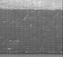
SEM cross-section of Ni/Al multilayer. Each layer is 25 nm thick
We are patterning materials at length scales smaller than what has been previously possible using two approaches. The first approach uses self-assembly principles. Our group has combined this method with plasma etching for preparing regular arrays of nanopillars and nanopores. Based on this approach, we have initiated a project in nano-engineering of substrates for nanocrystal growth. The second approach uses sophisticated electron-beam lithography, with resolution around 10 nm. Both techniques are being applied to such diverse areas as optoelectronics, magnetics, and energetics. We have used these approaches to engineer surfaces for photonic devices. In one demonstration, we have produced systematic changes in optical properties of semiconductors, silicon is shown. We are now experimenting with this method for altering device properties such as insertion and extraction efficiencies and beam shaping.
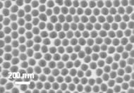
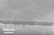
SEM micrographs of non-lithographic nanopores etched in silicon
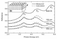
Optical reflectance vs nanopore depth
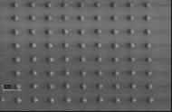
Metallic nanodots formed by electron-beam lithography.
Research Support: NSF–NIRT
Nano Tech Center
-
Address
Texas Tech University | Whitacre College of Engineering -
Phone
806.742.3533 -
Email
webmaster.coe@ttu.edu