
Materials Characterization Center - Specifications
Equipment List
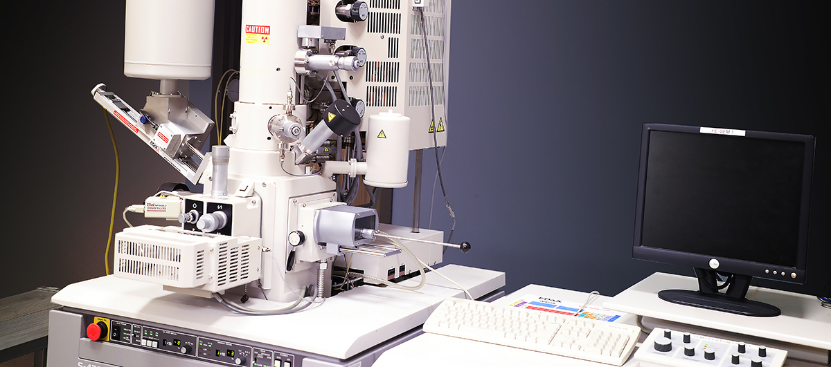
Hitachi S-4700 Field Emission Scanning Electron Microscope (FE-SEM) equipped with EDAX Energy Dispersive X-ray Spectrometer (EDS)
Imaging and Analytical Modes
- SEM secondary electron (SE) imaging of topography, morphology, and fine surface structure (at low <2 kV accelerating voltage)
- EDS elemental mapping and semi-quantitative composition analysis from millimeter to micrometer level
Features
- Cold field emission electron gun
- Accelerating voltage: 0.5 – 30 kV
- Magnification: up to 500,000x
- Secondary electron image resolution:
- 2.5 nm at 2 kV
- 1.5 nm at 15 kV
- Sample size: up to 25 mm diameter
- Sample tilt: -5 – +45°
- Sample rotation: 360°
- WD: 2.5 – 27.5 mm
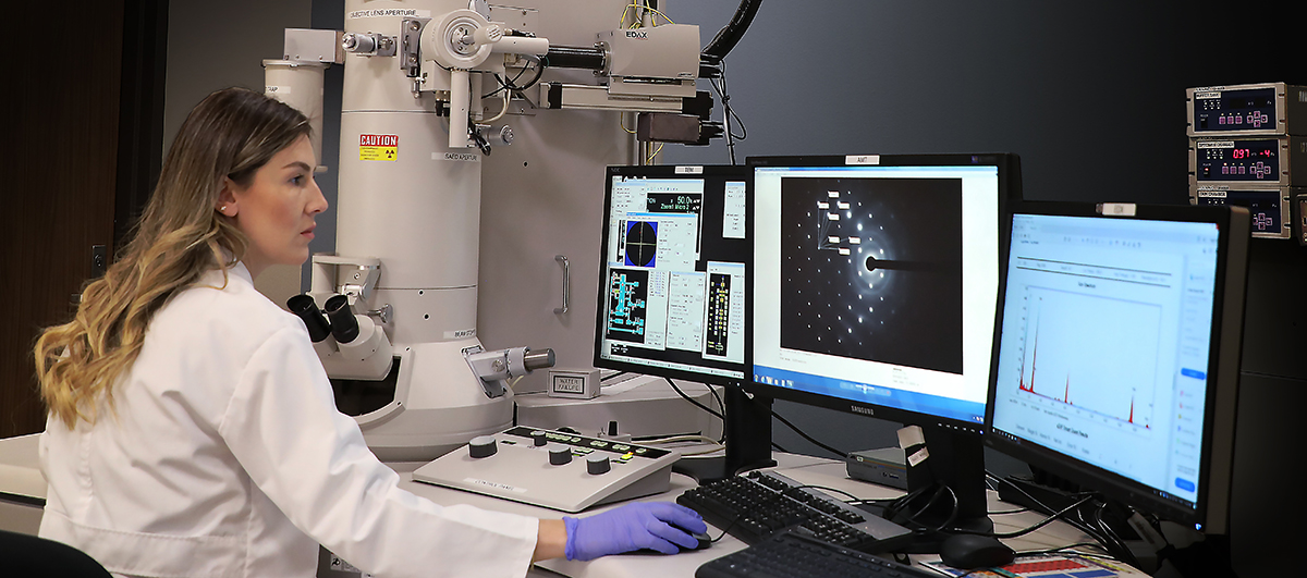
Hitachi H-9500 Transmission Electron Microscope (TEM) equipped with EDAX Energy Dispersive X-ray Spectrometer (EDS)
Imaging and Analytical Modes
- TEM bright field and dark field imaging, and selected area electron diffraction (SAED)
- Determine the internal structure of materials
- Crystalline: lattice fringes, SAED spots (single crystals) or SAED concentric rings (polycrystalline materials)
- Amorphous: no lattice fringes, no SAED patterns
- Determine the microstructure of materials
- Grain size
- Defects
- Dislocations
- Local microstructure (interfaces, individual nanostructures)
- Determine the internal structure of materials
- EDS elemental mapping and semi-quantitative composition analysis from micrometer to nanometer level
Features
- Electron gun filament: LaB6
- High resolution TEM: 0.10 nm (lattice), 0.18 nm (point-to-point)
- Accelerating voltage: 300 kV, 200 kV, 100 kV
- Magnification: up to 1,500,000
- Hitachi single tilt holder (tilt α = ±15°)
- Hitachi double tilt holder (tilt α = ±15°, β = ±15°)
- Hitachi in-situ gas injection heating holder
- TEM grid size: 3mm diameter
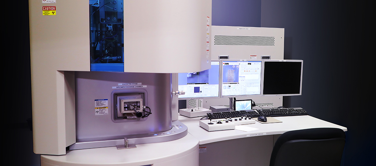
Hitachi NB5000 Focused Ion & Electron Beam (FIB-SEM) System equipped with EDAX Energy Dispersive X-ray Spectrometer (EDS)
Typical Uses and Applications
- FIB – used for site-specific material removal or deposition
- Removal = Sputtering/Milling
- Create site-specific cross-sections of materials for in-situ viewing be SEM in defect
analysis, materials characterization
- Mill and Monitor (automated process, use SEM to record images of thin slices incrementally milled by FIB)
- Site-selective TEM sample preparation (use SEM to monitor preparation of sample cross-section
by FIB)
- Prepare micro-sample from the original sample
- Lift-out micro-sample onto FIB grid (micro-sample carrier) with micro-sampling probe
- Thin micro-sample to ~100 nm thickness for TEM observation
- Create site-specific cross-sections of materials for in-situ viewing be SEM in defect
analysis, materials characterization
- Deposition
- W films – to protect sample surface during FIB processing, bond micro-sample to micro-sampling probe
- C films – use before W deposition to preserve sample surface features
- Removal = Sputtering/Milling
- SEM – used for sample imaging, enables the use of ED
- Imaging at 30 kV for thinned (~100 nm) TEM samples using STEM detector
- EDS elemental mapping and semi-quantitative composition analysis from millimeter to micrometer level
Features
- Vertical Ga+ ion column (FIB)
- Electron column tilted at 58° to vertical (SEM)
- FIB accelerating voltage: 1 – 40 kV
- SEM accelerating voltage: 0.5 – 30 kV
- SEM magnification: up to 800,000x
- Eucentric stage: SEM-style sample holder, max. sample size: 30mm diam.
- Side entry stage: TEM-style sample holder, sample size: 3mm diam.
- FIB-SEM holder compatible with TEM
Asylum Research MFP-3D-SA Atomic Force Microscope (AFM)
Analytical Modes and Applications
- Analytical Modes
- AC Mode Imaging in Air – Repulsive Mode (intermittent contact mode) – for imaging hard materials and polymers
- AC Mode Imaging in Air – Attractive Mode (non-contact mode) – imaging dried biological (soft) materials that should not be perturbed
- Contact Mode – for imaging hard materials
- Uses and Applications
- Imaging of topography
- Measure nanoscale surface roughness
- Measure nanoscale step height
- Determine size distribution of deposited nanoparticles
- Conductive AFM (CAFM) imaging – measurement of electrical behavior of thin films (current
passing through a sample and a tip is sensed)
- Determine conductivity
- Force spectroscopy – measurement of the deflection of the cantilever on the sample
surface
- Determine the interaction force between the tip and the sample surface
- Imaging of topography
Features
- AFM scanning in air
- Closed-loop, low noise, high precision scanner
- Max. scan size: 90 x 90 μm
- Max. vertical range: 24 μm
- Sub-angstrom vertical resolution
- Lateral resolution is limited by tip geometry, not the instrument
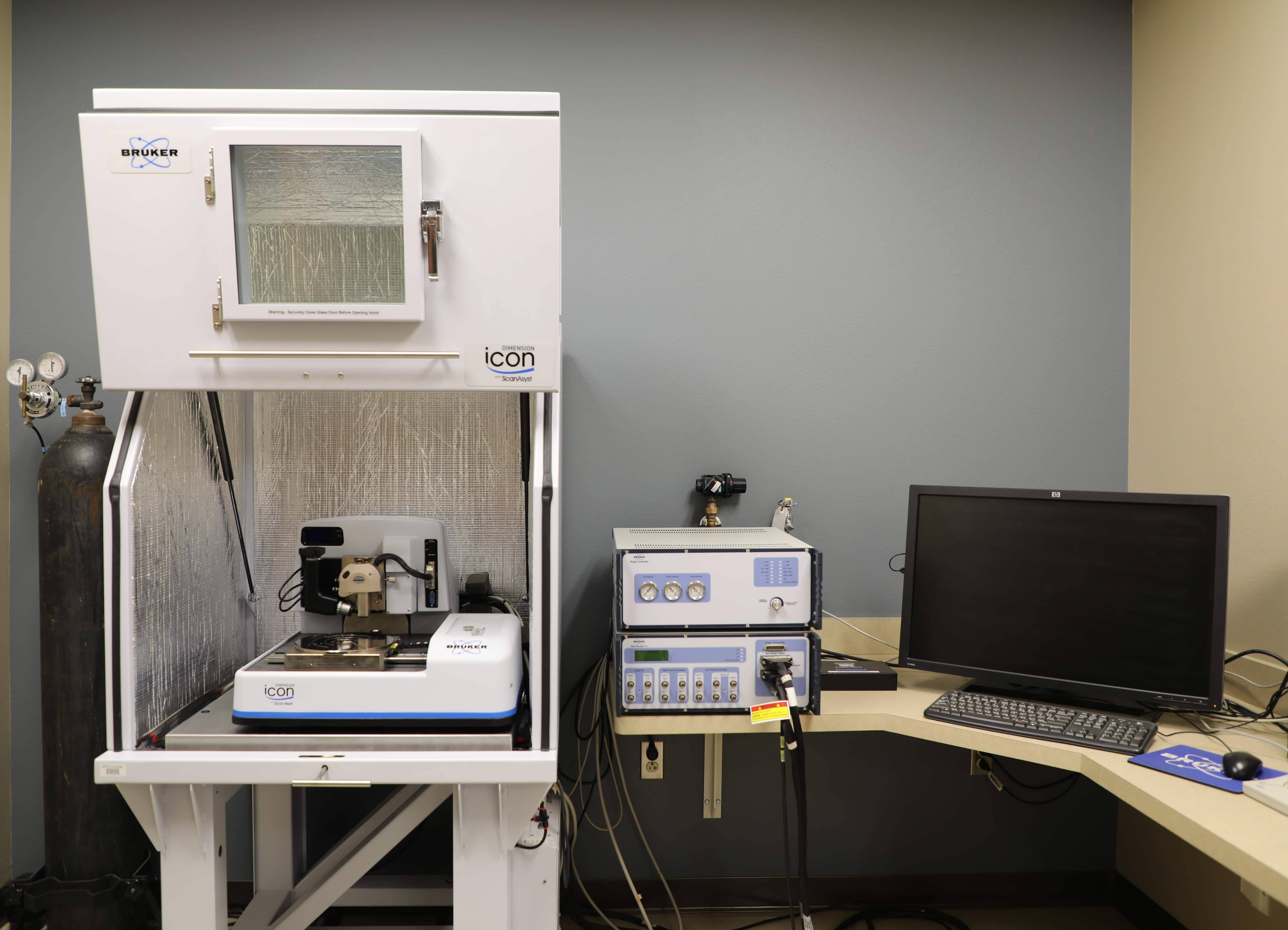
Bruker Dimension Icon with ScanAsyst Atomic Force Microscope (AFM)
Analytical Modes and Applications
- Analytical Modes
- Tapping Mode in Air – for imaging hard materials and polymers
- Contact Mode in Air – for imaging hard materials
- Contact Mode in Fluid – for imaging hard materials and biological materials
- ScanAsyst Mode (enables auto-optimization of scanning parameters)
- ScanAsyst and PeakForce Tapping Mode in Air
- ScanAsyst and PeakForce Tapping Mode in Fluid
- Uses and Applications
- Imaging of topography
- Measure nanoscale surface roughness
- Measure nanoscale step height
- Analysis in fluid cells and in controlled environments
- Imaging of topography
Features
- AFM scanning in air and in liquids
- Closed-loop, low noise, high precision scanner
- Max. scan size: 90 x 90 μm
- Max. vertical range: ~7 μm
- Sub-angstrom vertical resolution
- Lateral resolution is limited by tip geometry, not the instrument
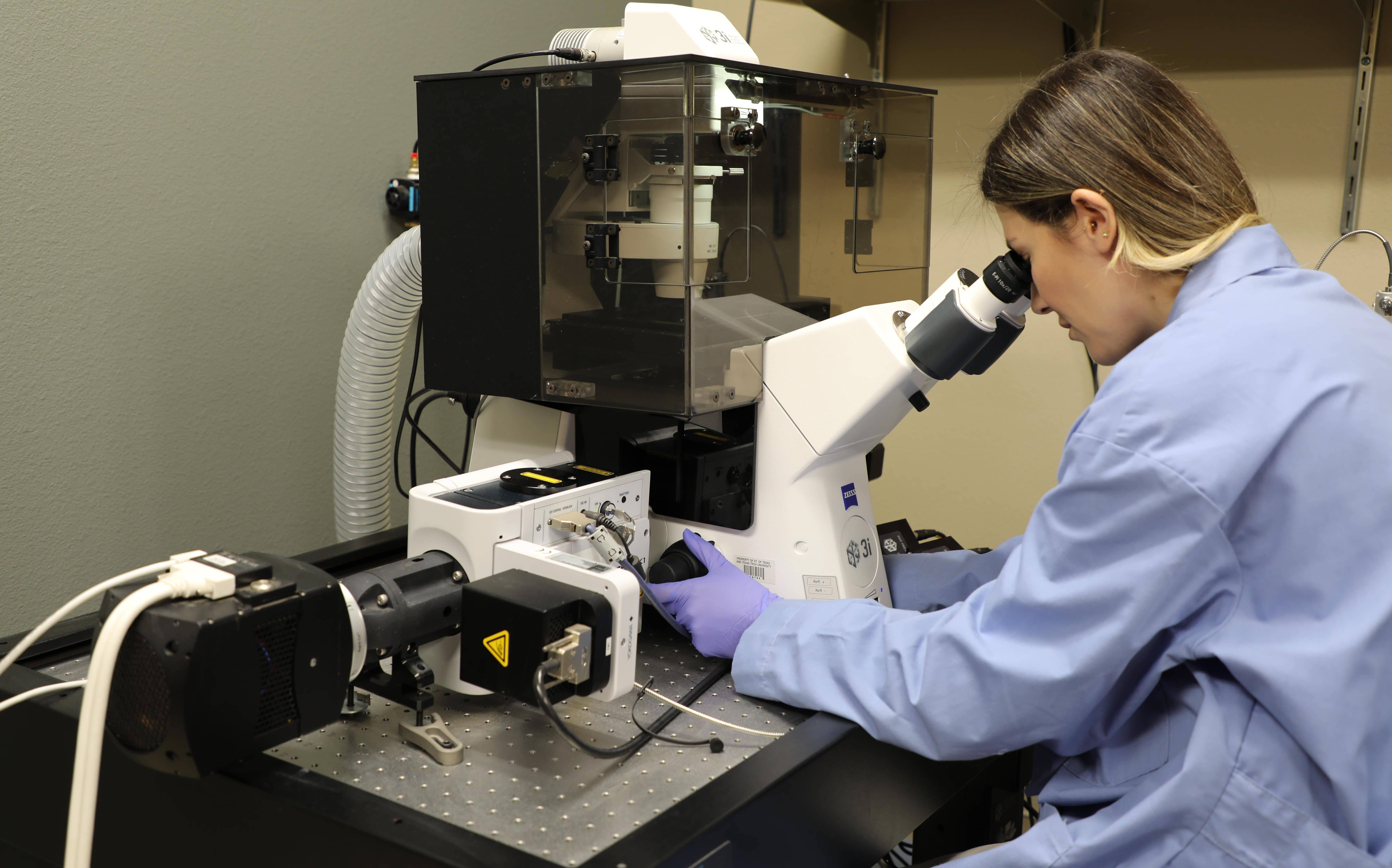
3i Marianas Spinning Disk Confocal System
Capabilities
- System is an optical microscope that uses fluorescence to generate an image
- aqueous specimens, live or fixed cells, either fluorescent samples or samples marked with fluorescent molecules
- System is a confocal fluorescence microscope
- Eliminates (blocks) out-of-focus signal in image formation, only in-focus signal is
used
- Increased resolution in the sample depth direction
- Captures multiple 2D images at different depths in a sample (optical sectioning) and reconstructs 3D structures
- Allows direct, noninvasive, serial optical sectioning of intact, thick living specimens with minimum sample preparation
- Eliminates (blocks) out-of-focus signal in image formation, only in-focus signal is
used
Features
- Yokogawa CSU-X1 Spinning Disc with CSUX1FW high-speed filter wheel
- Zeiss Axio Observer Z1 Inverted Microscope with motorized X, Y, Z Stage
- X-Cite 200DC Illumination System (340 – 800 nm filter)
- Okolab Full Enclosure Incubator with Temperature Control
- Fluorescent filter sets: DAPI, GFP and TxRed
- Lasers: 488 nm (blue) and 561 nm (green)
- Objectives: 5x Air, 10x Air, 20x Air, 40x Oil, 63x Oil, 100x Oil
- Evolve EMCCD Camera for fast imaging
- Software: SlideBook
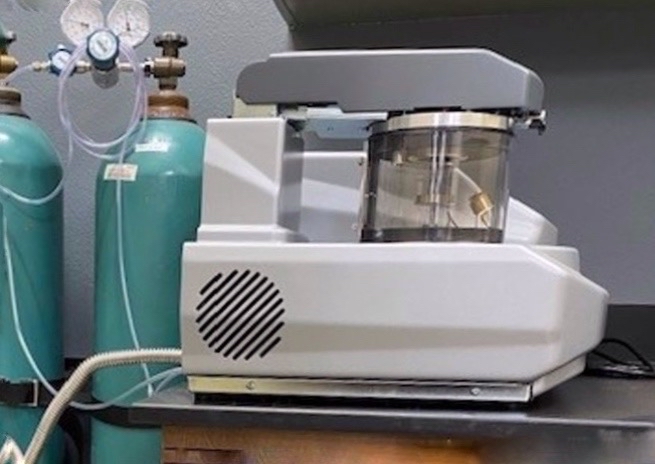
EMS Q150V ES Plus Sputter & Carbon Coater
Capabilities
- Combined system capable of both metal sputtering and carbon evaporation
- Cool magnetron metal sputtering using Au, Au/Pd (80/20), Pt, Cr, Ir targets
- Carbon rod evaporation
- Sputter coater is typically used for producing uniform metal coating on the surface
of the specimen to improve SEM results
- Inhibit charging effects
- Reduce thermal damage
- Improve secondary electron emission
- Coating
- To a predetermined thickness (use film thickness monitor)
- By a build-in timer
Features
- Fully automated coating process
- Scroll pump
- Turbomolecular pump
- Ultimate vacuum: 1 x 10˄-6 mbar
- Equipped with Film Thickness Monitor
Nikon Eclipse ME600D Metallurgical Microscope
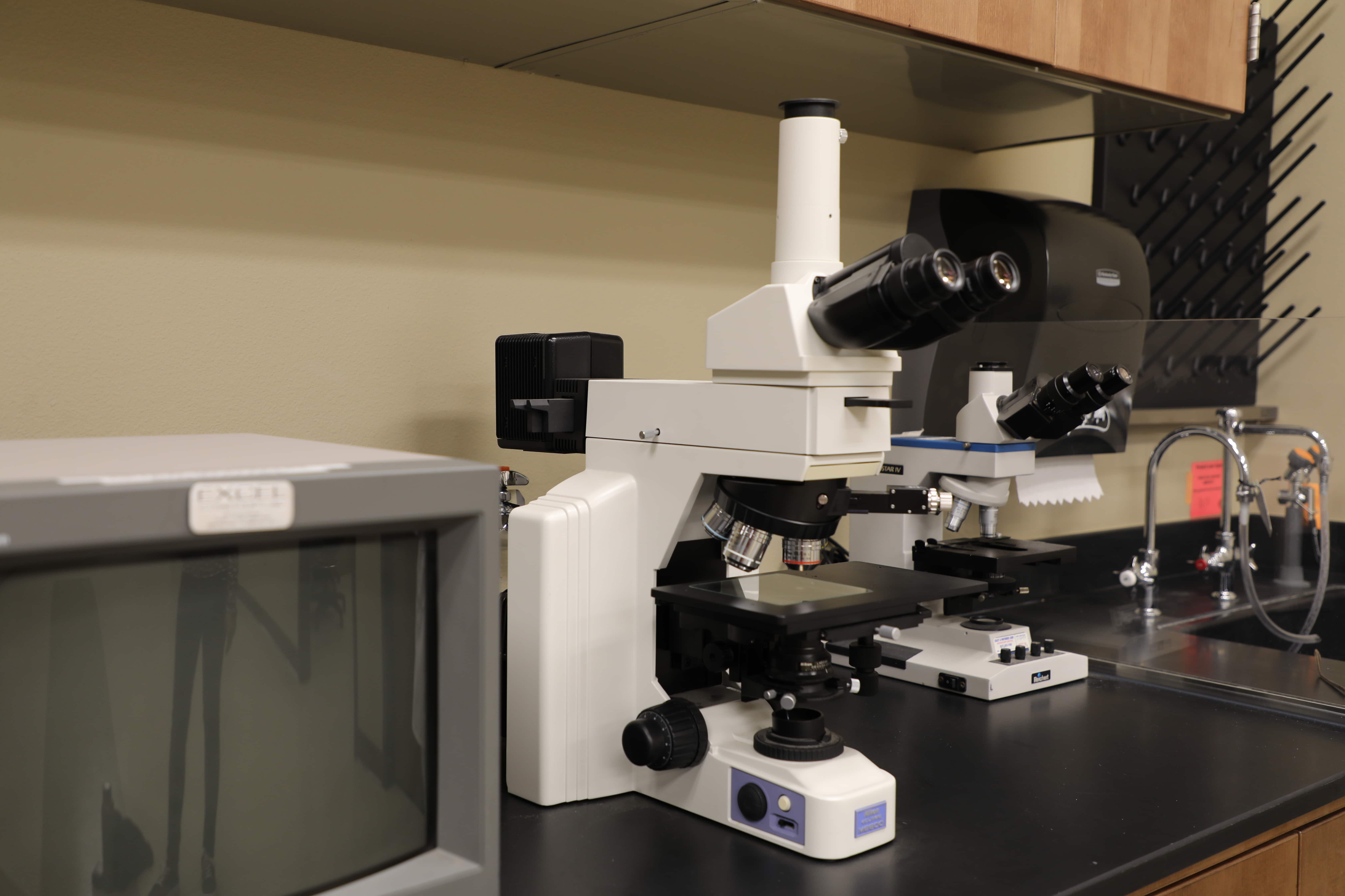
Features
- Uses white light as a light source
- Eyepieces: 10x
- Objective lenses: 5x, 10x, 20x, 50x, 100x
- Manual stage
- Techniques
- Brightfield (BF)
- Darkfield (DF)
- Differential Interference Contrast (DIC)
- Illumination – Reflected (EPI), Transmitted (DIA)
- Nikon CooPix950 digital camera for image capture
Nikon SMZ800 Stereoscopic Zoom Microscope
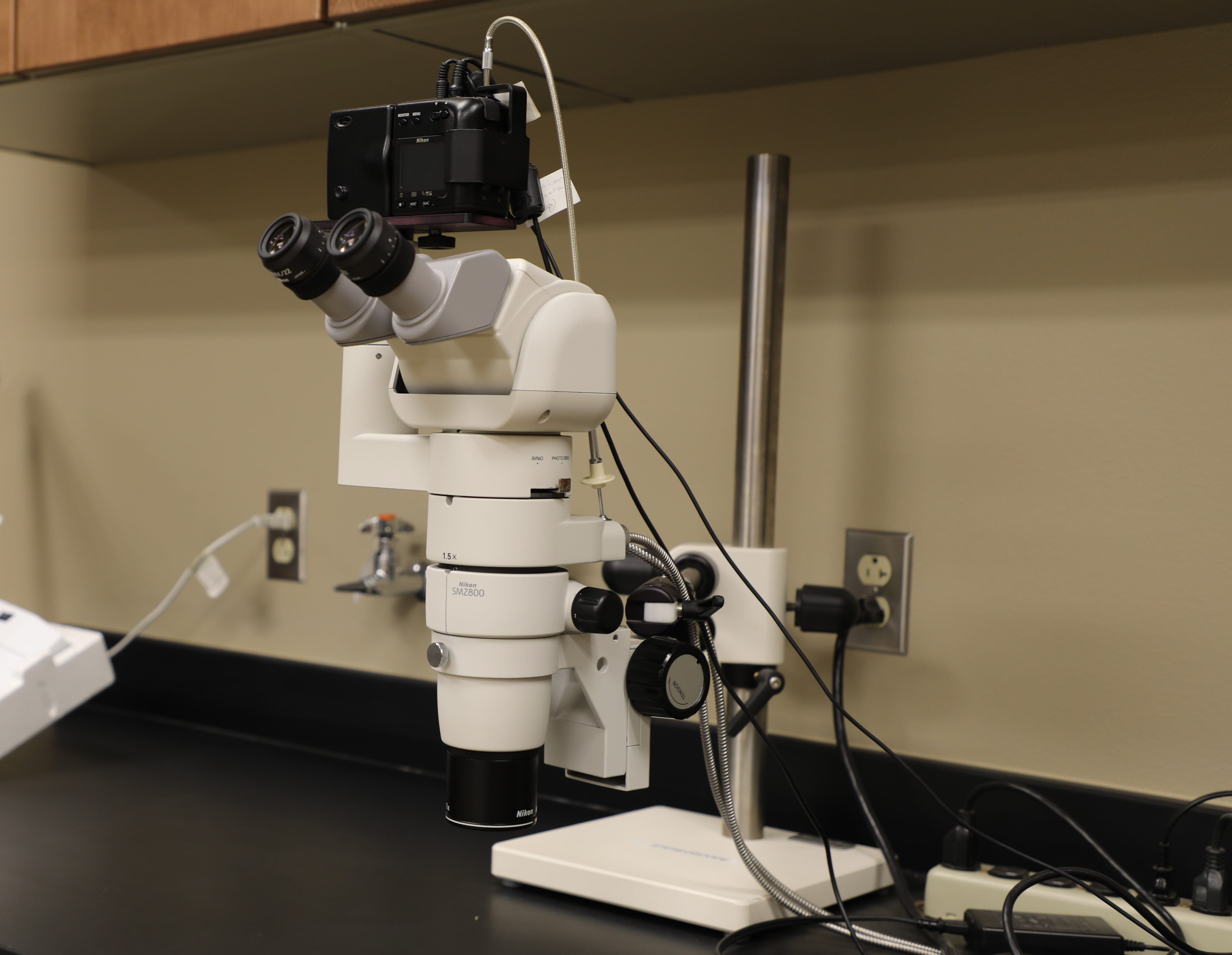
Features
- Stereomicroscope (3D visualization of a sample)
- Uses white light as a light source
- Eyepieces: 10x
- Objective lenses: Plan Apo 1x
- Total magnification: 10x – 63x
- Working Distance (WD): 78 mm
- Reflected (EPI) illumination
- Nikon CooPix950 digital camera for image capture
Rigaku MiniFlex 6G X-ray Diffractometer
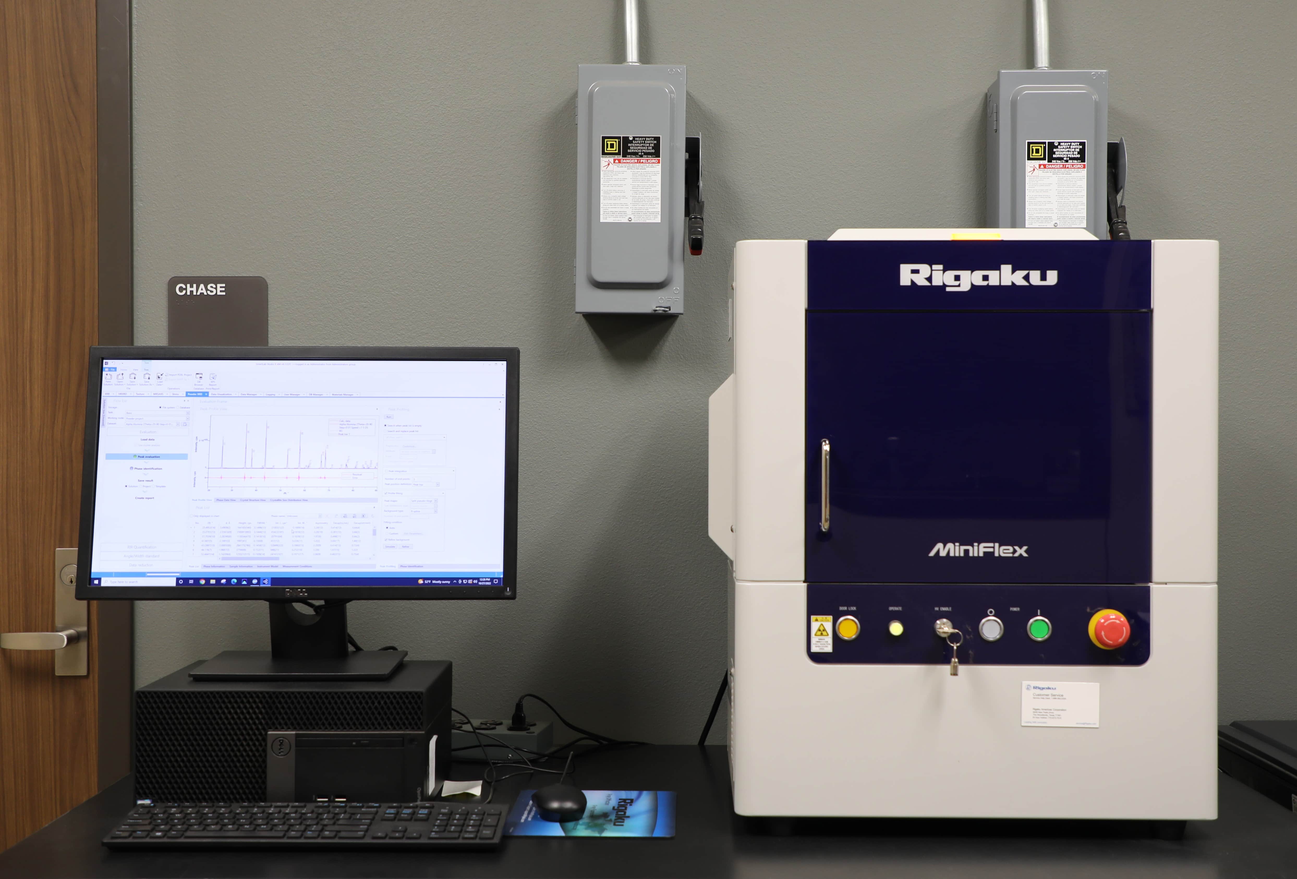
Typical Applications
- Powder samples
- Non-monochromatized Cu Kα radiation
- SmartLab Studio II software to analyze XRD data
- Phase identification
- Phase composition (wt% of the phases present in the sample) determination
- Lattice parameter refinement
- Crystallite size and lattice strain determination
- % Crystallinity determination
Features
- Benchtop X-ray diffractometer
- Cu X-ray tube (Cu Kα radiation)
- D/teX Ultra high speed 1D detector
- Vertical θ/2θ goniometer with a horizontal sample mount
- Standard sample stage
- ASC-8 automated sample changer with spinner
- SmartLab Studio II software
Rigaku SmartLab 3kW XE X-ray Diffractometer
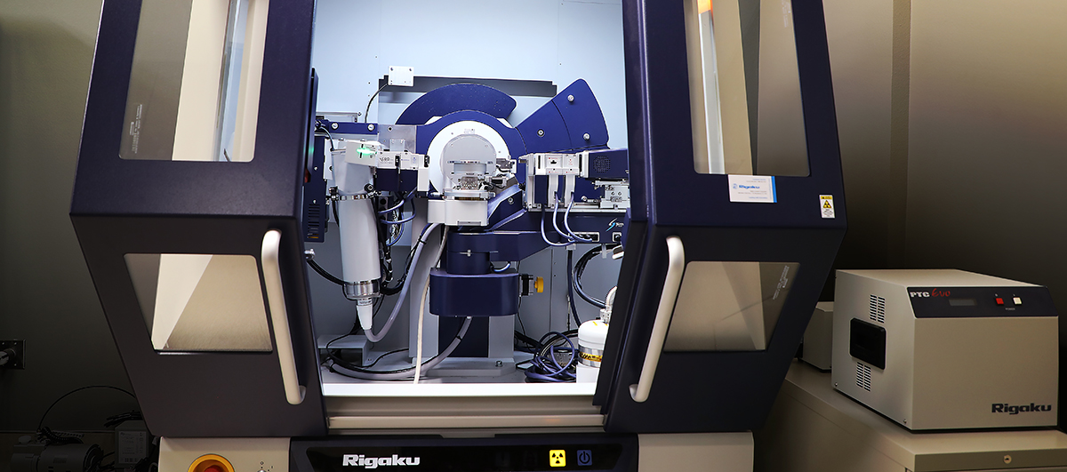
Typical Applications
- Powder samples – use Bragg-Brentano (divergent beam) optics
- Low angle XRD (Min. 0.5 °2θ) – for materials with a long-range order
- In-situ high-temperature XRD analysis for phase transitions
- Thin film samples – use parallel beam optics and Cu Kα or Cu Kα1 radiation
- Grazing incidence XRD (GIXRD) – for very thin films
- Pole figure measurement – determine sample texture
- High resolution XRD (HRXRD) – use Cu Kα1 radiation for near-perfect crystals, epitaxial
films to improve resolution
- Rocking curve (w-scan) – study defects in films (e.g., mosaic spread, curvature, misorientation)
- 2θ-w coupled scan – study lattice mismatch, composition, strain/relaxation
- X-ray reflectivity (XRR) – determine layer(s) thickness, density, and roughness
- Residual stress analysis of polycrystalline samples – use high 2θ angles (> 120 °2θ)
- Transmission small angle X-ray scattering (SAXS) analysis of powder samples in capillaries
- Determine the particle or pore size distribution
- Micro area mapping – mapping of sample phase composition requiring spatial resolution of 500 and 100 μm
Features
- General purpose XRD system
- Cu X-ray tube
- HyPix-3000 high energy resolution 2D detector
- Vertical θ/θ goniometer with a horizontal sample mount
- Ge(220) 2 bounce crystal monochromator
- Sample plates: 4” Wafer, Height reference, Transmission SAXS
- Attachment heads: Standard, RxRy, XY 20 mm
- Attachment bases: Standard, ASC-6, φ, χφ
- Multipurpose high-temperature attachment (RT-1500 °C)
Physical Electronics PHI 5000 VersaProbe II Hybrid X-ray Photoelectron Spectrometer (XPS)
Capabilities
- Surface analysis (analysis depth < 10 nm)
- Determine sample elemental composition
- Determine oxidation (bonding, chemical) states of specific element
- Sputter depth profiling (manual or programmable) – determine the composition change
of a thin film along the entire film thickness
- Series of spectra acquired at different sample depths after material was sputtered with Ar+ ions
- Angle resolved XPS – determine the composition change of a thin film at the near surface
region without sputtering
- Sample is tilted between 90° – 5° with respect to the electron energy analyzer. Analysis depth decreases with the decreasing sample tilt angle.
- Map acquisition – 2D display of elemental information
- Map consists of an array of individual pixels. A complete spectrum is collected at each pixel.
- Typically use Al X-ray source, but if Auger peaks overlap photoelectron (XPS) peaks
can use Mg X-ray source to separate them
- Photon energy of Al Kα = 1486.6 eV, photon energy of Mg Kα = 1253.6 eV (Difference = 233 eV)
- Shift Auger peaks positions by 233 eV, while XPS peaks positions remain unchanged on the binding energy scale
Features
- Monochromatic Al X-ray source (FXS)
- Achromatic Mg X-ray source (Conventional source)
- Electron energy analyzer
- Electron neutralizer
- Ar+ ion gun
- High vacuum: ~10˄-8 Pa (roughing pumps, TMPs, Ion pump, Titanium sublimation pump)
- Analysis spot: 10 – 100 μm
Bruker Optics VERTEX 70 Fourier Transform Infrared (FTIR) Spectrometer/HYPERION 2000 Infrared (IR) Microscope
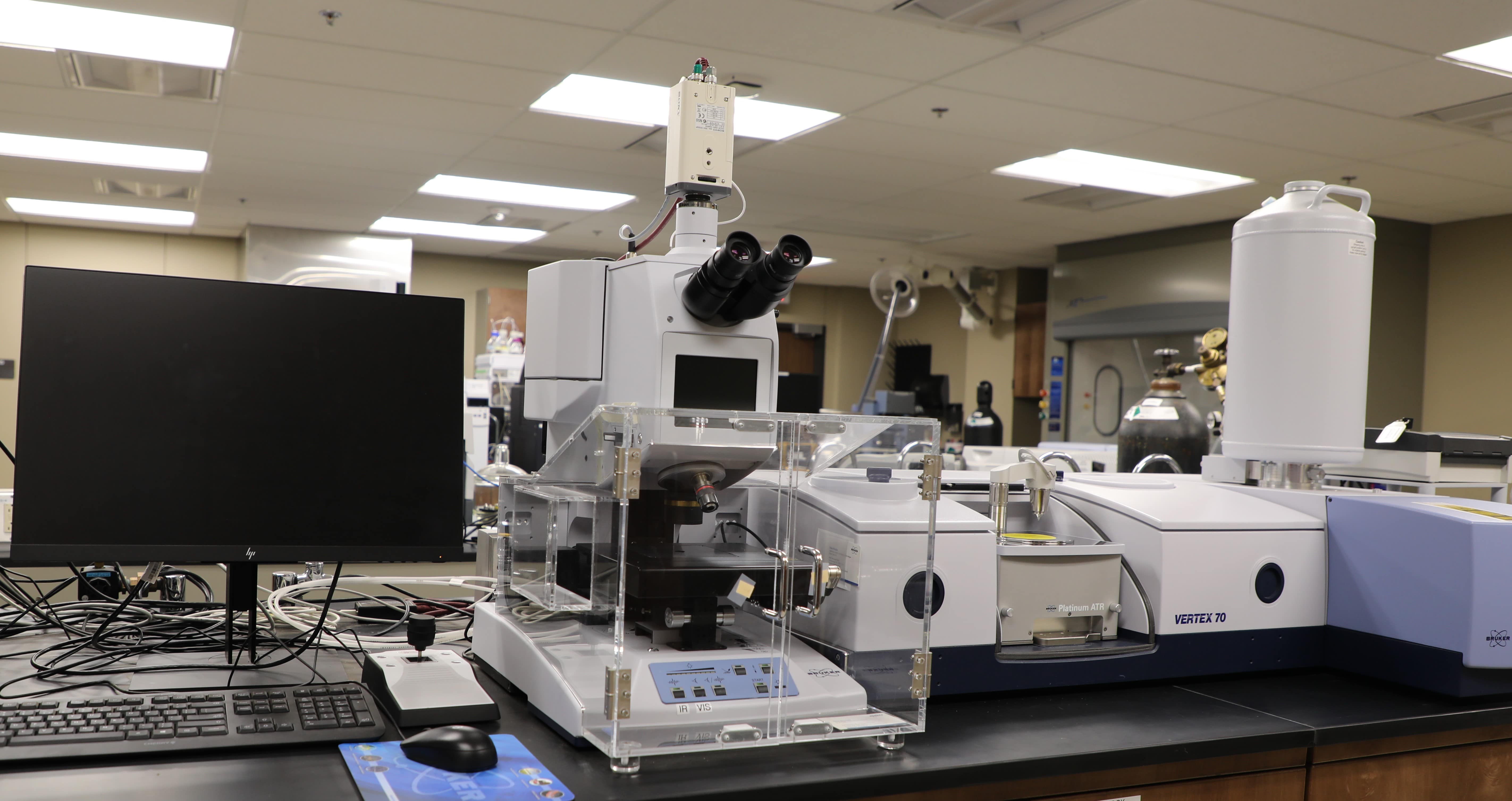
Capabilities
- Study and identify chemical substances or functional groups in solids and liquids
- VERTEX 70 FTIR Spectrometer – for bulk samples
- Transmittance accessory (MIR = 8,000-350 cm-1, NIR = 12,800-5,800 cm-1)
- For sufficiently thin and transparent solids (need to be pressed into thin pellets) and liquids
- HARRICK Praying Mantis DRIFTS accessory (MIR = 4,000-400 cm-1)
- For powders/ground samples, may need to dilute sample with KBr
- Bruker Optics Platinum ATR (diamond crystal) accessory (MIR = 8,000-350 cm-1, NIR
= 10,000-5,800 cm-1)
- For strongly absorbing, black, thick samples
- Liquids, solids, powders, rubber, pastes, gels, creams, films, surface coatings
- Only thin layer (~0.5 – 2 μm) is analyzed
- Transmittance accessory (MIR = 8,000-350 cm-1, NIR = 12,800-5,800 cm-1)
- Hyperion 2000 IR microscope – for micro samples, small sample areas, examination of
inhomogeneities in heterogeneous samples
- 15x objective – for transmittance and reflectance (MIR = 8,000-600 cm-1, NIR = 10,000-2,000
cm-1)
- Transmittance mode – for sufficiently thin and transparent samples
- Reflectance mode – for solid samples with very smooth surfaces
- 20x ATR II (Ge crystal) objective – for ATR (MIR = 5,000-600 cm-1, NIR = 5,000-2,000
cm-1)
- ATR mode – for strongly absorbing, black, thick solid samples
- Only thin layer (~0.5 – 2 μm) is analyzed
- 15x objective – for transmittance and reflectance (MIR = 8,000-600 cm-1, NIR = 10,000-2,000
cm-1)
Features
- VERTEX 70 FTIR spectrometer (resolution: 0.4 cm-1)
- MIR source, KBr beamsplitter, RT DLaTGS detector
- NIR source, CaF2 beamsplitter, RT InGaAs detector
- Analysis spot: ~1.6 x aperture size
- Transmittance, DRIFTS, ATR accessories
- Hyperion 2000 IR microscope (resolution: 0.4 cm-1)
- MIR source, KBr beamsplitter, LN2-cooled MCT detector
- NIR source, CaF2 beamsplitter, LN2-cooled MCT detector
- 15x objective (Min. analysis spot: 15 μm)
- 20x ATR II objective (Analysis spot: 5 – 100 μm)
- PIKE Crush IR hydraulic press with pellet press
Bruker Optics RAM II Fourier Transform Raman (FT-Raman) Spectrometer / RamanScope III FT-Raman Microscope / Senterra Dispersive Raman Microscope Spectrometer
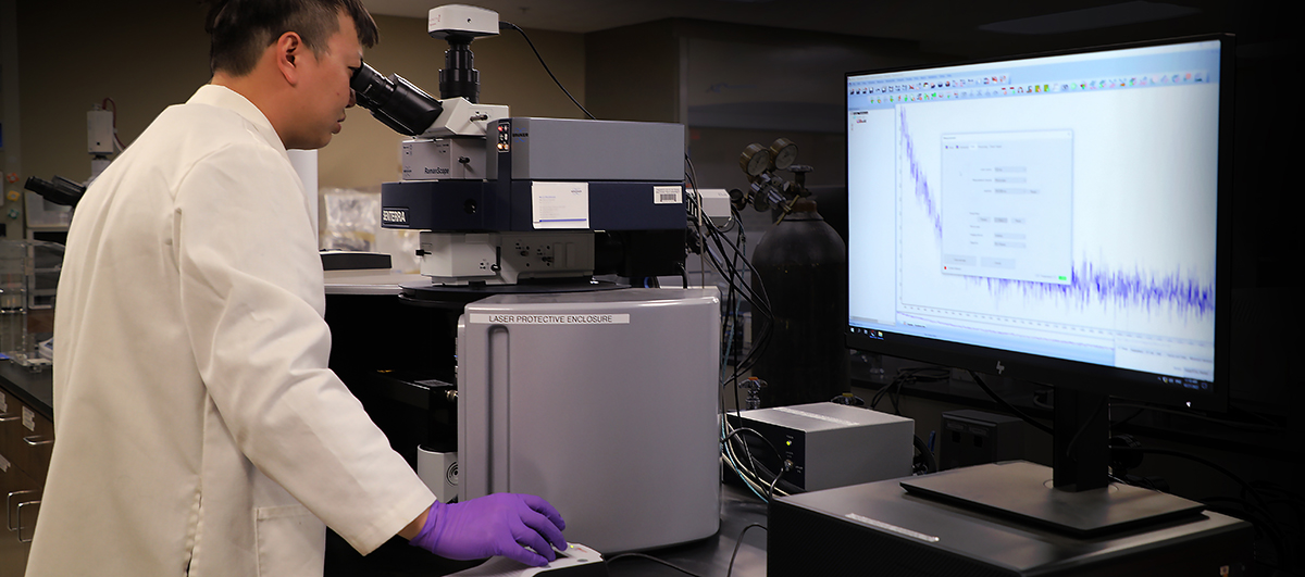
Capabilities
- Study and identify chemical substances or molecular structures in solids and liquids
- Senterra Dispersive Raman Microscope Spectrometer
- 532 nm laser, spectral range 50 – 3,700 cm-1
- 785 nm laser, spectral range 100 – 3,500 cm-1
- For samples, which do not fluoresce when exposed to laser radiation in visible range
- Micro samples, small sample areas, examination of inhomogeneities in heterogeneous samples
- Chemical mapping or surface scan – acquire spectra at predefined measurement positions arranged by moving the sample in x- and y-direction using a motorized stage
- Depth profiling – acquire spectra at the same x, y measurement position but in different predefined sample layers by moving the laser focus incrementally deeper into the sample
- 3D map – combination of surface scan and depth profiling
- RAM II FT-Raman spectrometer and RamanScope III microscope
- For samples, which tend to fluoresce when exposed to laser radiation in visible and UV range
- Spectrometer – for bulk samples
- Microscope – for micro samples, small sample areas, examination of inhomogeneities in heterogeneous samples
Features
- RAM II FT-Raman spectrometer / RamanScope III microscope
- 1064 nm Nd:YAG laser (500 mW)
- NIR LN2-cooled Ge detector
- NIR CaF2 beamsplitter
- Spectral resolution: 0.8 cm-1
- 40x objective (microscope)
- Senterra Dispersive Raman Microscope Spectrometer
- 785 nm (100 mW) and 532 nm (20 mW) lasers
- Thermoelectrically cooled CCD detector
- Spectral resolution: 3-5 cm-1
- 4x, 20x, 50x objectives
Agilent/Varian Cary 5000 UV-Vis-NIR Spectrophotometer
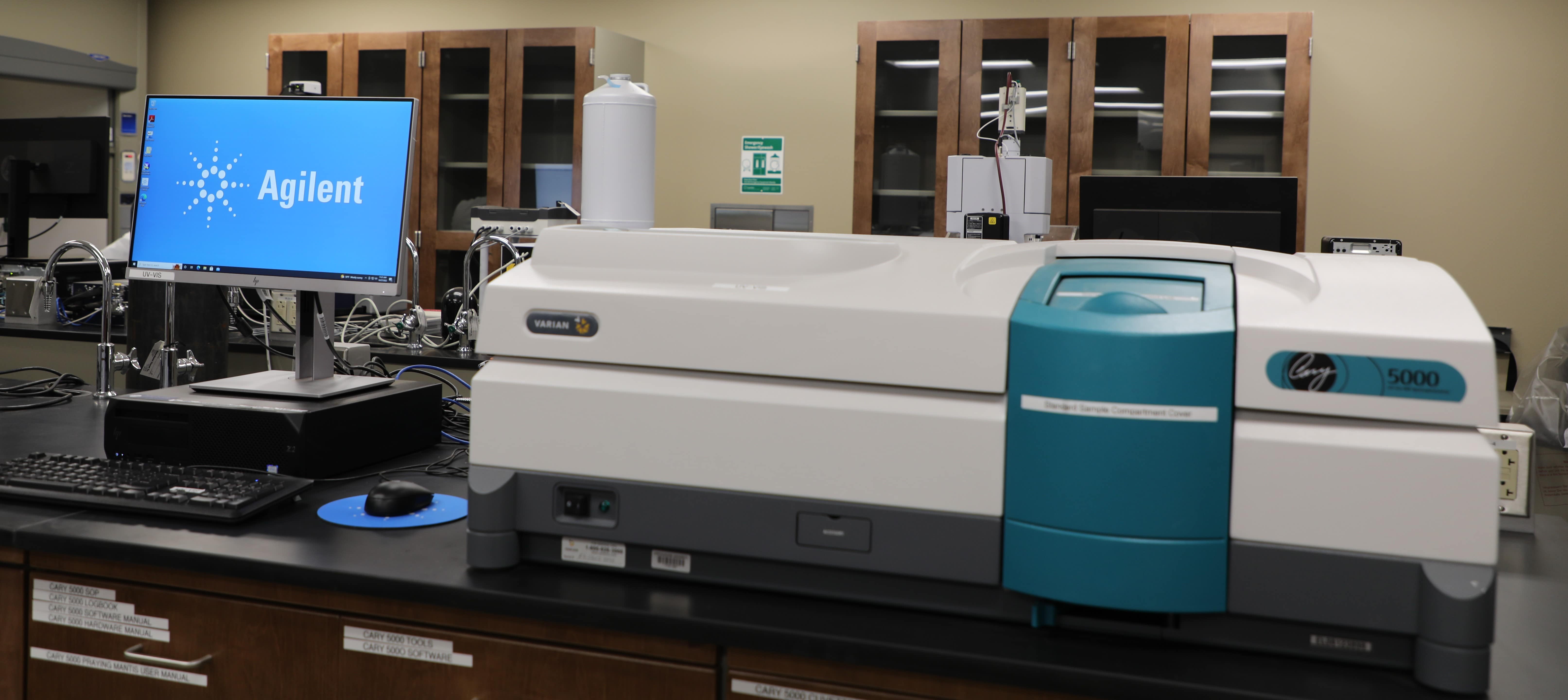
Capabilities
- Determine optical properties of materials (solids, liquids)
- Need the sample and the reference (baseline) spectra
- Powders
- Use the HARRICK Praying Mantis diffuse reflectance accessory and matching sampling
cups for the reference and the sample
- Reference = Spectralon (PTFE powder)
- Sample = Sample of interest
- Use the HARRICK Praying Mantis diffuse reflectance accessory and matching sampling
cups for the reference and the sample
- Thin films
- Use thin film sample holder and matching solid sample slides for the reference and
the sample
- Reference = Substrate alone
- Sample = Film on substrate
- Use thin film sample holder and matching solid sample slides for the reference and
the sample
- Liquids
- Use liquid sample holder and matching cuvettes for the reference and the sample
- Quartz cuvettes – transparent in the UV/Vis range
- Glass cuvettes – transparent in the Vis range
- Plastic cuvettes – noise below 250 nm
- Reference = solvent alone
- Sample = solute + solvent
Features
- Deuterium lamp – for the UV region
- Halogen lamp – for the Vis/NIR region
- Spectral range: 200 nm – 3000 nm
- Different accessories/holders for powders, thin films, liquid
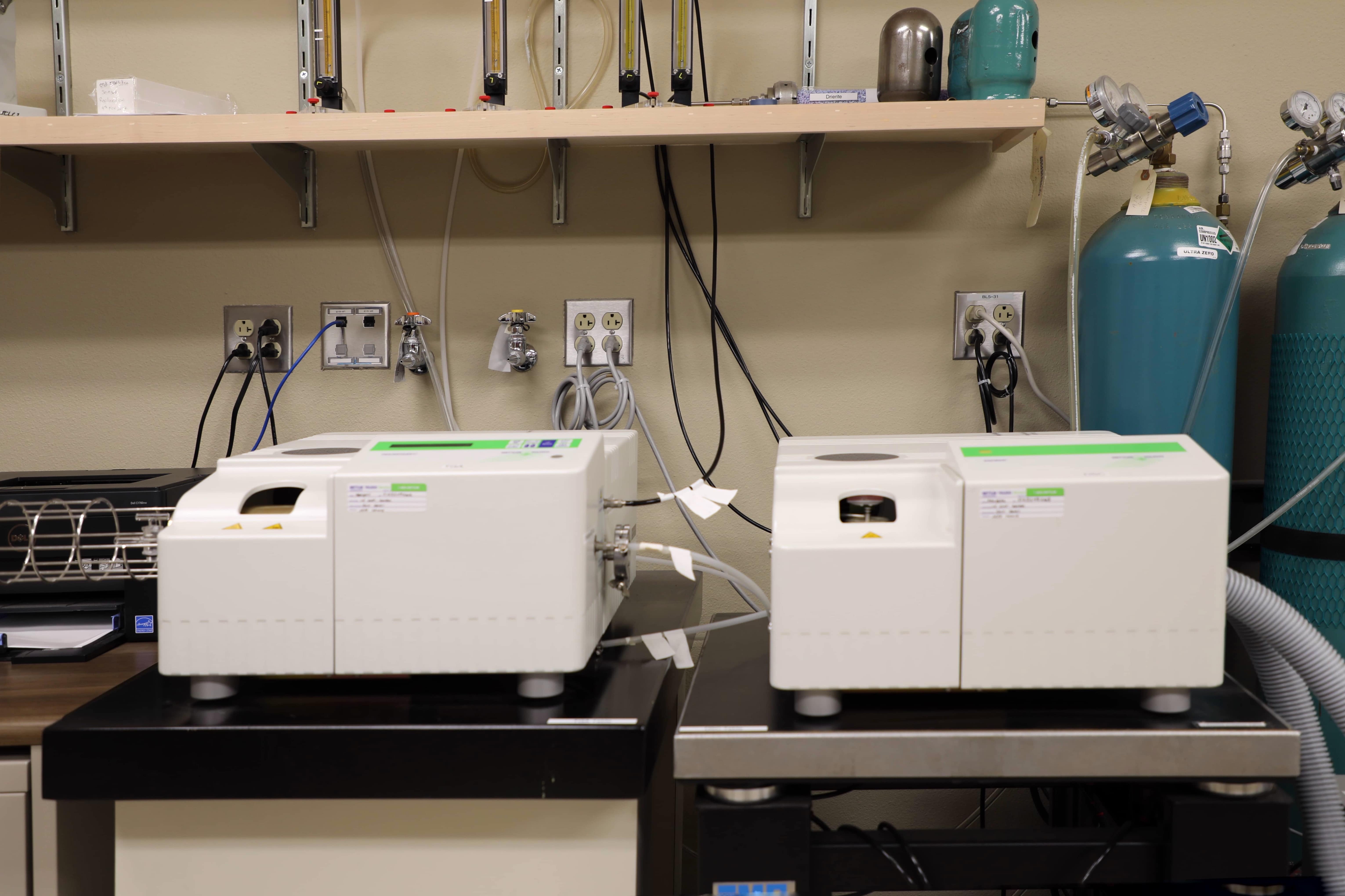
Agilent 7820A Gas Chromatograph (GC) – 5977B Mass Selective Detector (MSD) System
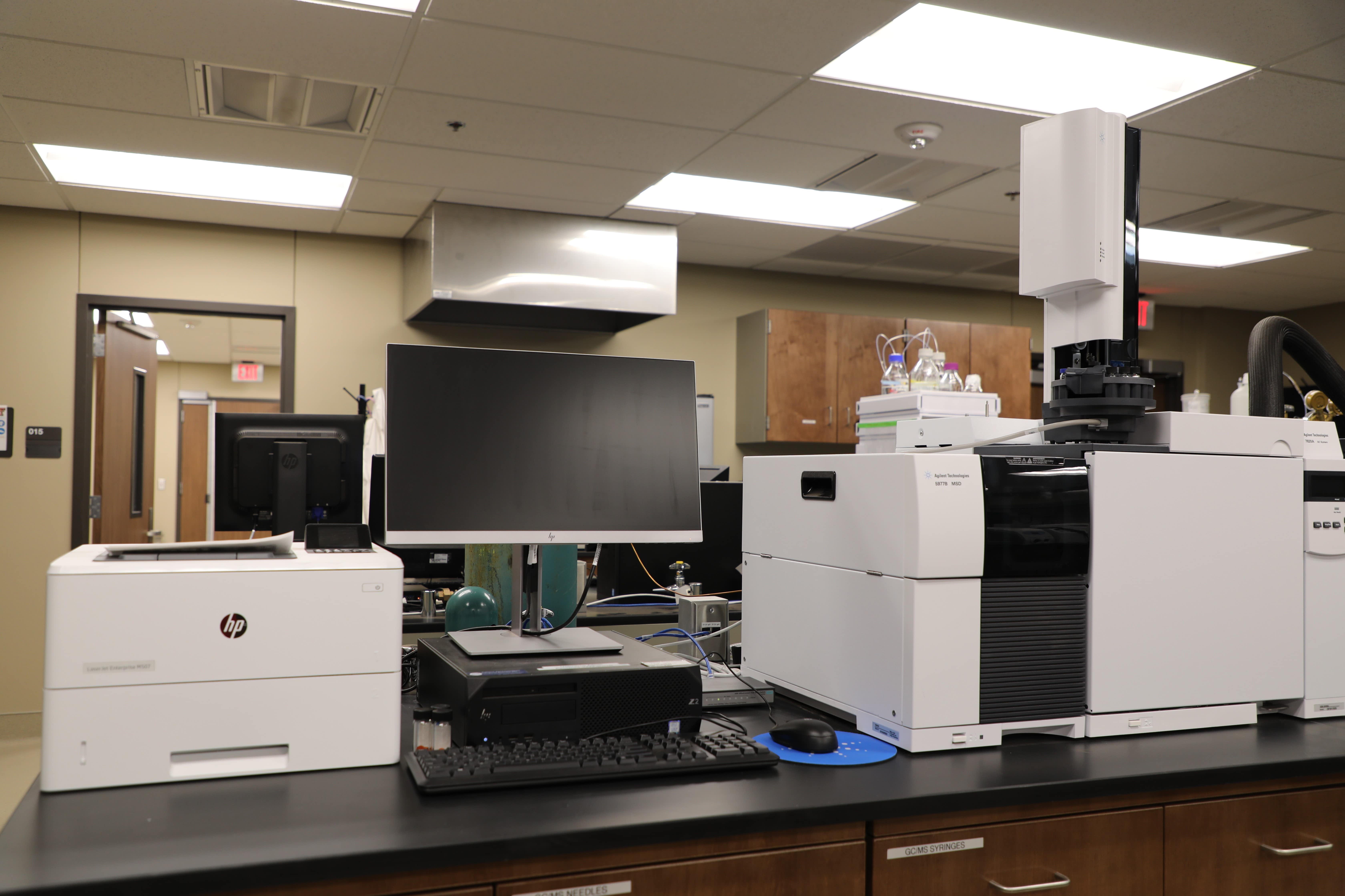
Features
- Split/Splitless (SSL) inlet for all capillary columns
- Automatic Liquid Sampler (ALS)
- 16 vial turret
- Detector:
- Mass Selective Detector (MSD)
- Instrument Detection Limit (IDL): 24 fg
- Ionization mode: Electron ionization (EI)
- Stainless steel source
- Ion source temperature: 150–350 °C
- Quadrupole temperature: 106–200 °C
- Micro-Ion vacuum gauge
- Column: Capillary Column
- Carrier: Helium
- Software:
- GCMS MassHunter
- MS Quantitative Analysis
- Library: NIST 2014 MS
Microtrac Zetatrac Ultra Zeta Potential and Particle Size Analyzer
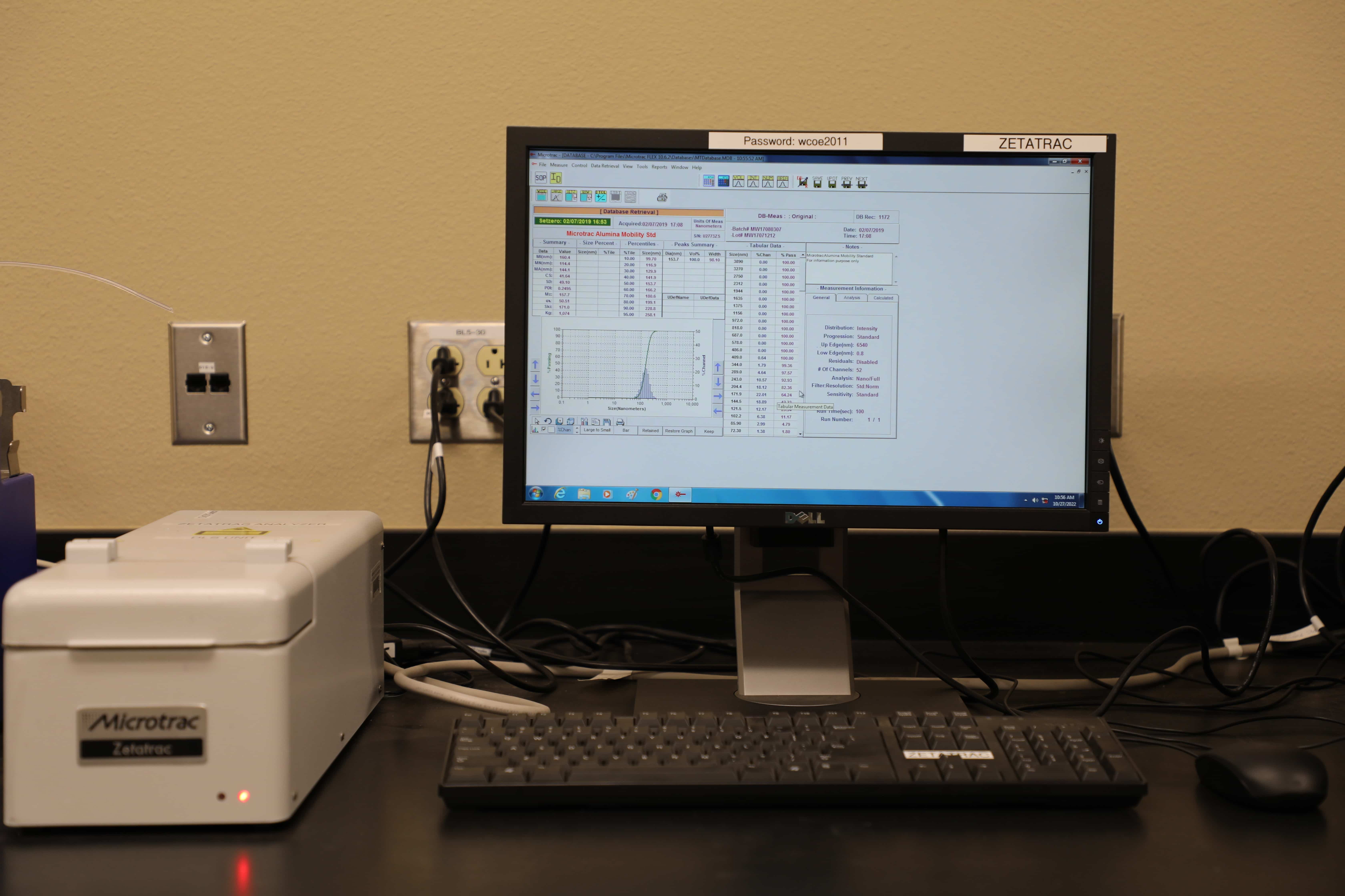
Capabilities
- Determination of the particle size distribution of particles suspended in water and other liquids
- Light source: two 3 mW Laser Diodes, wavelength 780 nm
- Principle of operation: dynamic light scattering (DLS)
- Need to provide
- Particle refractive index, shape (spherical, irregular), transparency (transparent, absorbing, reflecting)
- Dispersing liquid viscosity and refractive index
- Need to provide
- Need to have well dispersed particles
- Use water, surfactants, solvents, ultrasonication
- Measurement range: 0.8 nm – 6.54 μm
- Size: hydrodynamic diameter = the equivalent spherical diameter of a particle with the same translational diffusion coefficient as the measured particle
- pH range: 3 – 11
- Min. sample volume: 3 mL
- Measurement temperature: 20 °C – 30 °C
- Sample concentration: must be within the optimal range determined by the instrument
- Software: Microtrac FLEX
TSI API Aerosizer Particle Size Analyzer
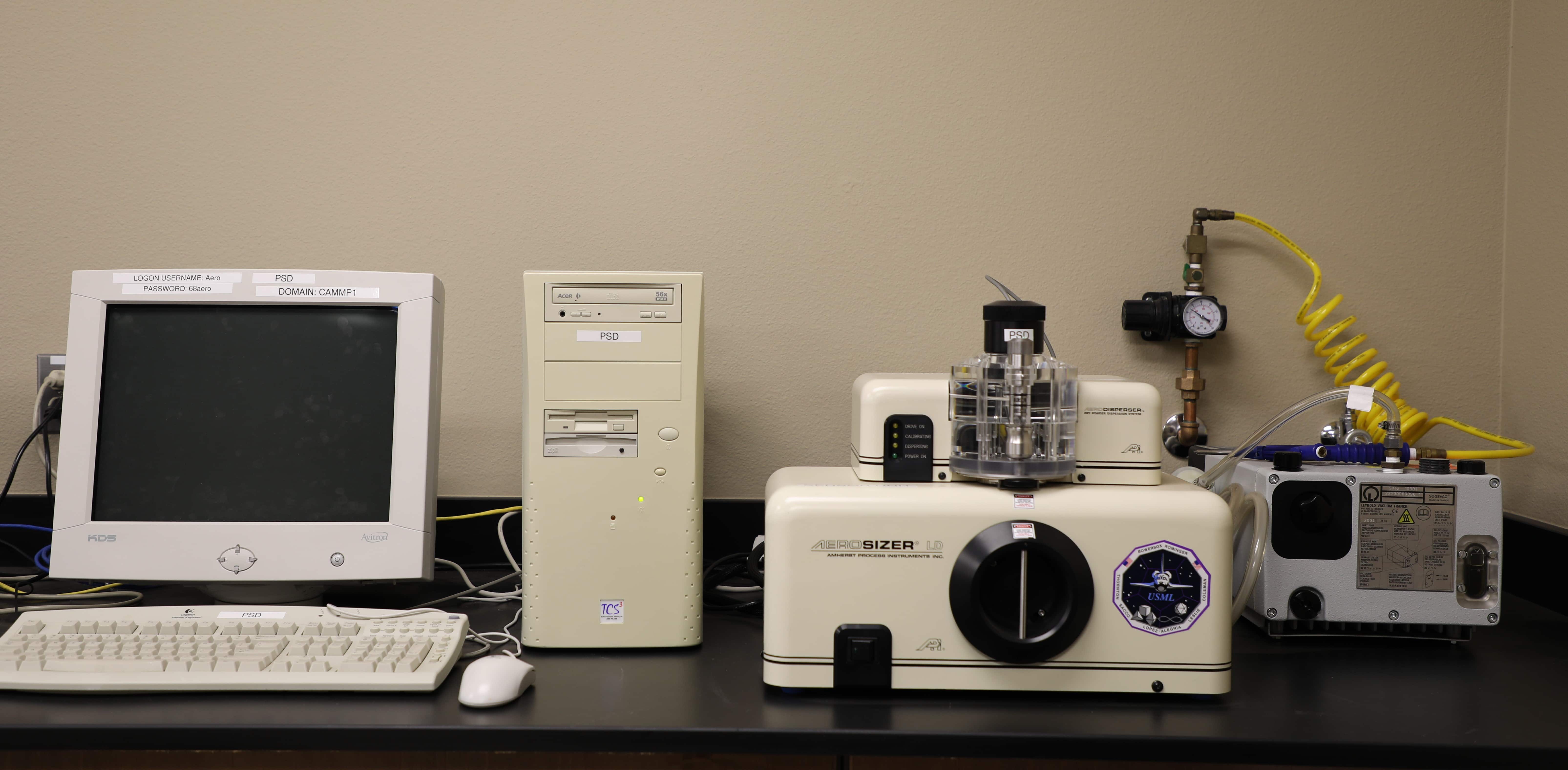
Features
- Determination of the particle size distribution of dry powders suspended in flowing air
- Model: Aerosizer LD
- Light source: 3 mW Laser Diode
- Principle of operation: Aerodynamic time-of-flight
- Need to provide material density
- Aero-Disperser accessory: dry powder dispersing system
- Advanced fluidization, controlled de-agglomeration and proprietary transonic flow dispersion technology
- Very good results for both “free flowing” and “highly cohesive” powders
- Measurement range: 200 nm – 700 μm
- Size: geometric diameter = the equivalent spherical diameter of a particle with the same density as the measured particle
Quantachrome Autosorb iQ (ASiQ) Micropore Analyzer
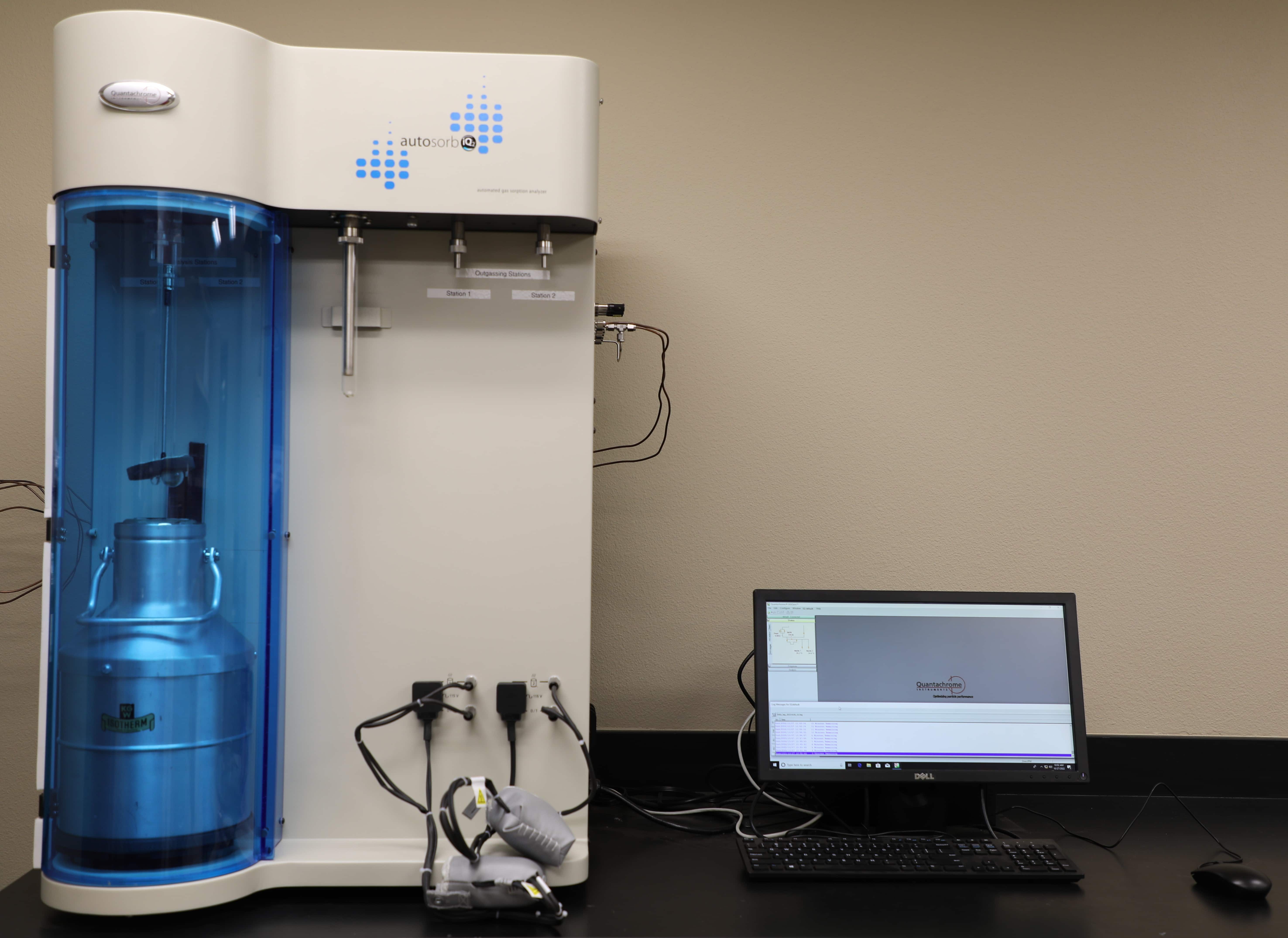
Features
- Determination of the specific surface area, pore volume, and pore size distribution of microporous and mesoporous materials
- Automated gas sorption analyzer
- Adsorbate gas: Nitrogen
- Measurement temperature: LN2 boiling point (77.4 K)
- Two outgassing stations
- Two physisorption stations
- 6 mm, 9 mm, 12 mm physisorption cells
- 90,000 rpm TMP backed by dry diaphragm pump
- Outgassing temperature: up to 350 °C
- Software: ASiQwin
Particle Metrix Stabino Particle Charge Mapping System
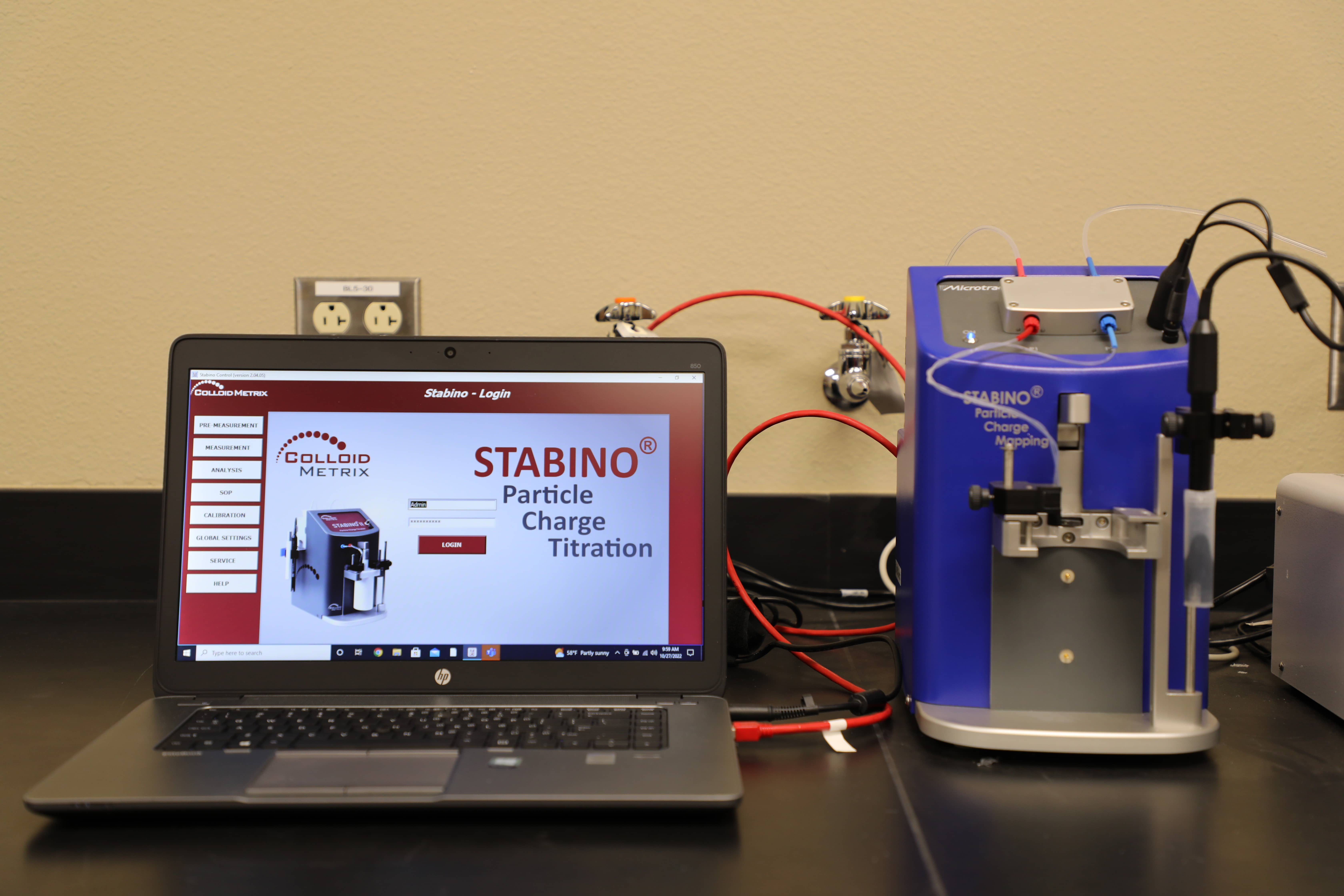
Features
- Measurements of particles suspended in aqueous and other polar media
- Principle of operation: measurement of streaming potential
- Sample (particles + dispersing medium)
- Particle size: < 100 μm
- Volume: 10 mL
- Concentration: 0.001 – 70 wt% or 0.001 – 40 vol%
- pH: 2 – 12 (pH measurements only in aqueous media)
- Titrant
- Aqueous media only (to avoid damage of the pH electrode)
- Volume: 0 – 20 mL
- Min. single titration step: 10 μL
- pH: 2 – 12
Mettler Toledo DSC822e module Differential Scanning Calorimeter
Features
- Measure the difference between the heat flows to the sample and reference crucible as a function of temperature
- Temperature range: -150 – 700 °C
- Measurements in: Dry air or Nitrogen
- Crucible size: 40 μL
- Max. heating rate: 100 K/min
- Temperature accuracy: ±0.2 °C
- Resolution: 0.04 μW at RT
- LN2 cooling to -150 °C
Edward E. Whitacre Jr. College of Engineering
-
Address
100 Engineering Center Box 43103 Lubbock, Texas 79409-3103 -
Phone
806.742.3451 -
Email
webmaster.coe@ttu.edu